Supporting imagery
Models
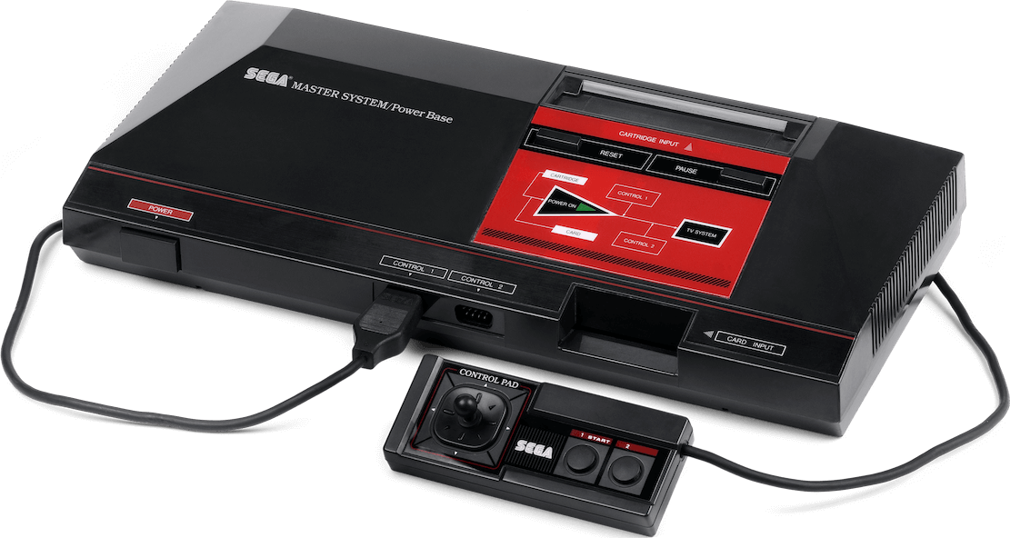
Released on 20/10/1985 in Japan, 09/1986 in America and 06/1987 in Europe
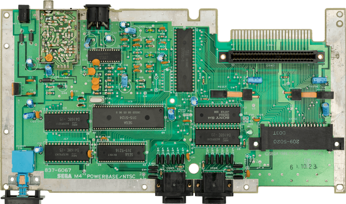
Motherboard
The sound chip is embedded in the video display processor.
Diagram
A quick introduction
The Master System comes from a long line of succession. What began as a collection of off-the-shelf components has now acquired a new identity thanks to Sega’s engineering.
Models and variants
I was a bit confused at first when reading about the different models that Sega eventually shipped. So, here is a summary of the main models to clarify any potential confusion:
- Sega Mark III: The first console featuring this architecture, released exclusively in Japan.
- Sega Master System (Europe and America): A rebranded Mark III with a new case, a BIOS ROM chip, and a different cartridge slot.
- Sega Master System (Japan): A European/American Master System with the Mark III’s cartridge slot, a new FM chip, and a jack port for ‘3D glasses’. However, it lacks the
RESETbutton.
From now on, I’ll use the term ‘Master System’ or ‘SMS’ to collectively refer to these models, except when discussing features exclusive to a specific variant.
CPU
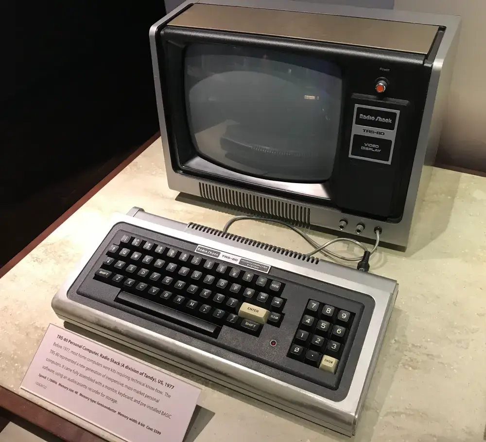
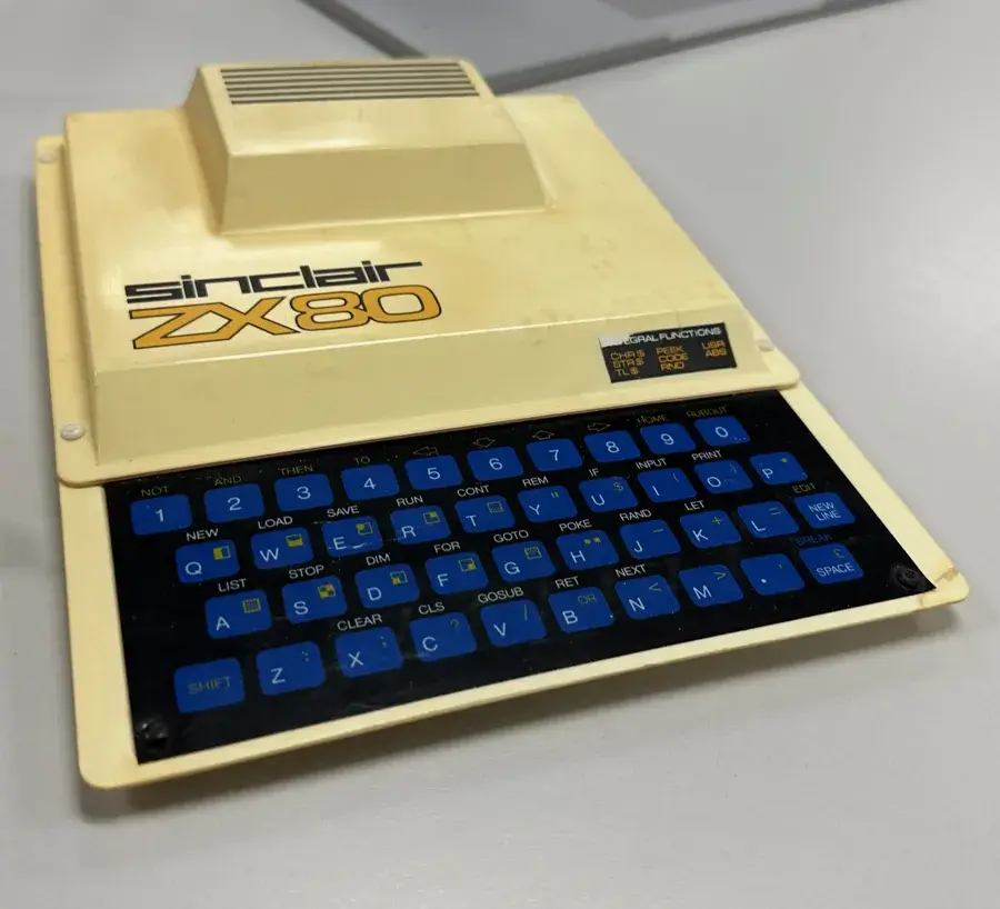
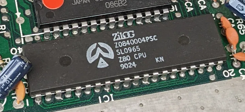
Sega opted for a fully-fledged Zilog Z80 CPU running at ~3.58 MHz, a popular choice among computer manufacturers such as Sinclair, Amstrad, and Tandy.
The Z80 CPU has an interesting background, as it was designed by none other than the authors of the Intel 8080 (Federico Faggin and Masatoshi Shima), who became disenchanted with Intel’s direction and decided to start their own silicon company, Zilog, in 1974.
Their debut product can be considered an unofficial successor to the Intel 8080, now featuring:
- The Z80 ISA: An instruction set compatible with the Intel 8080 but expanded with lots more instructions. It handles 8-bit words.
- An 8-bit data bus, ideal for moving 8-bit data around. Larger values will consume extra CPU cycles.
- Fourteen 8-bit general-purpose registers [2]: This is quite a lot, considering the Intel 8080 features half and the MOS 6502 only three. However, the Z80’s register file exhibits some caveats (or advantages, depending on how you see it):
- Only seven registers are accessible at a time, the other seven are called ‘Alternative Registers’ and must be swapped with the first set to be able to access them. This aligns with the principle of bank switching. Also, the Z80 provides specialised instructions like
EXandEXXto transfer the contents between each set. - Within each set, six 8-bit registers may also be paired together to provide up to three 16-bit registers, allowing the manipulation of larger values.
- Only seven registers are accessible at a time, the other seven are called ‘Alternative Registers’ and must be swapped with the first set to be able to access them. This aligns with the principle of bank switching. Also, the Z80 provides specialised instructions like
- A 16-bit address bus, its consequences are explained in the next section.
- A 4-bit ALU: This may be a bit shocking, but it simply means that operations on 8-bit values take twice as many cycles to compute.
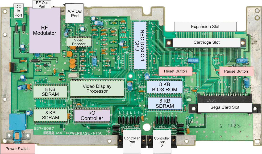
The motherboard picture at the start of the article shows an NEC D780C-1 CPU, which is simply SEGA second-sourcing the chip to different manufacturers. Other revisions even included the chip manufactured by Zilog. But for this article, it doesn’t matter who fabricated the CPU, as the internal features remain the same.
Relative comparison
Notice how the 6502 CPU (featured in the NES) runs at a mere ~2 MHz, which is about half the speed of the Master System’s chip. Combined with the Z80’s larger register file, one might assume the Master System would outperform the NES without a doubt.
Conversely, if we dig deeper, we see that the 6502 houses a larger (8-bit) ALU. Thus, arithmetic operations that may only take two cycles in the 6502, will consume four on the Z80. Ultimately, this shows that relative qualities like CPU clock speed or register file size, when analysed in isolation, may be deceiving. Both the Z80 and 6502 excel and struggle at different tasks; it all comes down to the skills of the programmer.
Memory available
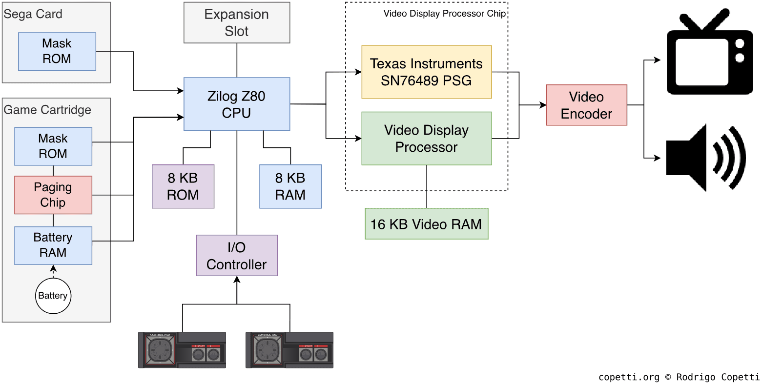
As mentioned earlier, the Z80 has a 16-bit address bus, so the CPU can find up to 64 KB worth of memory. Now, in the Master System’s memory map, you’ll find 8 KB of RAM for general-purpose use [3], this is mirrored in another 8 KB block. Finally, up to 48 KB of game ROM are mapped as well.
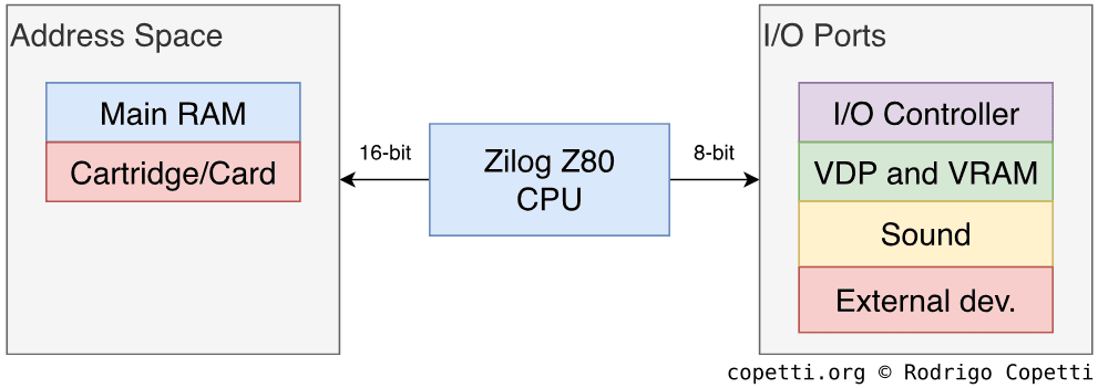
Accessing the rest of the components
As you may have read in the previous paragraph, only the main RAM and some cartridge ROM are found in the address space. So, how does the program access other components? Well, unlike Nintendo’s Famicom/NES, not all the hardware in the Master System is mapped to memory locations. Instead, certain peripherals are accessed through the I/O space.
This is because the Z80 family contains an interesting feature called I/O ports, which enable the CPU to communicate with other hardware without exhausting memory addresses. To achieve this, there is a separate address space for ‘I/O devices’ called ports, and both share the same data and address bus. The difference, however, is that ports are read from and written to using IN and OUT instructions, respectively, as opposed to the traditional load/store instruction (LD).
When an IN or OUT instruction is executed, the Z80 sets up the address lines to point to the peripheral (which could be, for instance, a keyboard), flags its IORQ pin to indicate that an I/O request has been initiated, and finally flags the RD pin or the WR pin depending on whether it’s an IN or OUT instruction, respectively. Consequently, the addressed peripheral must manually monitor the address bus and the I/O pins and perform the required operation. In the case of an IN instruction, the CPU stores the received value in a predefined register.
The way SEGA interconnected the CPU with the rest of the components enables it not only to access values but also to expose or conceal certain components from the memory map.
Interestingly, the Game Boy housed a Z80 ‘variant’ that completely omitted the I/O ports. Thus, it had to fit everything into the memory map.
Backwards compatibility
The architecture of this console is very similar to its predecessor, the Sega SG-1000. This allowed the Master System to gain backwards compatibility with the SG-1000. Although, this only applies to the Japanese variant, as others feature a different cartridge slot.
Graphics
The drawings on the screen are produced by a proprietary chip called Video Display Processor or ‘VDP’. Internally, it shares the same design as the Texas Instrument TMS9918 (used in the SG-1000) [4], though it has been enhanced with features which we will discuss in the following sections.
Organising the content
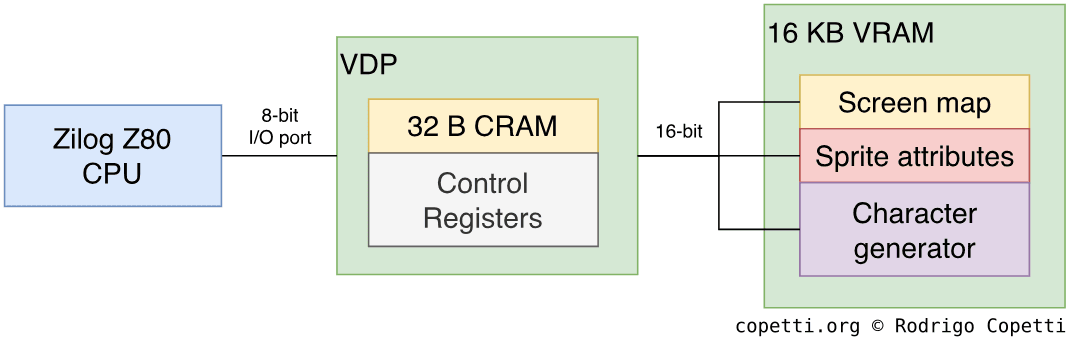
Connected to the VDP are 16 KB of VRAM, which only the VDP can access using a 16-bit data bus (Sega modified the original design to access two memory chips with 8-bit buses simultaneously [5]). If you look at the motherboard picture again, you’ll notice that both RAM and VRAM chips are roughly the same, except that VRAM uses the chip model ending in ‘20’, which offer lower latency [6].
For the Master System, VRAM houses everything the VDP requires for rendering (except Colour RAM). The CPU fills VRAM by writing to specific VDP registers, which in turn forward the values to VRAM. Since the VDP is accessed through I/O ports, the CPU must use IN and OUT instructions.
Constructing the frame
The VDP renders frames with a resolution of up to 256x192 pixels. Later revisions added support for 256x224 px and 256x240 px. However, to maintain compatibility with all models, developers adhered to the standard resolution. This chip has the same modus operandi as Nintendo’s PPU; in other words, graphics are rendered on the spot.
Furthermore, the VDP has four different modes of operation. These alter the characteristics of the frame (colour depth and resolution):
- Mode 0 to III: Inherited from the TMS9918 found on the SG-1000. They are included for backwards compatibility, although any SMS game can use them.
- Mode IV: The native mode of the Master System, which enables access to all the state-of-the-art features of the VDP. For this analysis, we will focus on this mode!
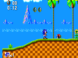
Let us now examine how a frame is drawn step by step. For this, I’ll borrow Sonic The Hedgehog’s assets. Also, to make explanations easier, this analysis will focus on the standard memory layout that Sega suggests for organising the graphics content (just remember that the VDP is very flexible, allowing games to optimise the layout).
Tiles

Mode IV is based on the tile system. To recall previous explanations about tile engines, tiles are just 8x8 pixel bitmaps that the renderer retrieves to draw the game’s graphics. In the case of the VDP, the frame consists of two planes: the background layer and the sprite layer.
Inside VRAM, there is an area dedicated to tiles called Character generator (Sega refers to tiles as ‘Characters’), and it’s set to be 14 KB long. Each tile occupies 32 bytes, so we can store up to 448 tiles.
Each tile contains 64 pixels, and the VDP rules that each pixel must use 4 bits, allowing 16 colours can be chosen. These bits reference a single entry in Colour RAM or ‘CRAM’, which is located within the VDP and stores the colour palettes. Colour palette systems reduce the size of tiles in memory and enable programmers to alternate their colours without storing multiple copies.
Colour RAM stores two palettes of 16 colours each. Each entry is 6 bits wide, with each 2-bit set defining one colour from the RGB model. This provides a total of 64 colours to choose from.
Background Layer
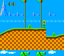
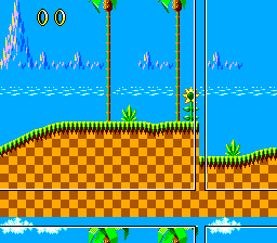
The background layer is a large plane where static tiles are drawn. To place something here, there is another area in VRAM called Screen map, which takes 1.75 KB.
This allows developers to build a layer of 896 tiles (32x28 tiles) [7], but if we do the math, we see that this layer is larger than the display resolution of the console. The reality is, only 768 tiles (32x24 tiles) are visible, so the visible area is manually selected at the programmer’s will. Also, by slowly alternating the X and Y coordinates of the selected area, a scrolling effect is achieved.
Each entry in the map is 2 bytes wide (matching the width of the VDP’s data bus) and contains the address of the tile in the Character generator, along with the following attributes:
- Horizontal and Vertical flip.
- The priority bit (determines whether to draw some or all the tile in front of sprites).
- The colour palette used.
Curiously enough, there are three unused bits in the entry that the game can use for other purposes (e.g., extra flags to assist the game engine).
Sprites
Sprites are essentially tiles that can move freely. The VDP can raster up to 64 sprites using a single tile (8x8 px) or two tiles stacked vertically (8x16 px).
The Sprite Attribute Table is a 256-byte area in VRAM that contains an array of all the defined sprites. Its entries are similar to those of the background layer, except that each sprite contains two additional values representing the X/Y coordinates.
The VDP is limited to a maximum of eight sprites per horizontal scan-line [8]. Also, if multiple sprites overlap, the first one in the list is displayed.
Result
The VDP automatically blends the two layers to form the final frame. The rendering process is performed scan-line by scan-line, so the VDP doesn’t really know how the frame will look; that’s only visible to the user once the picture is constructed on the TV.
If you examine the example image, you may notice a vertical column at the left side of the frame. This occurs because the screen map is tall enough to provide vertical scrolling without producing artefacts, but not wide enough for horizontal scrolling. To address this, the VDP can mask the left-most side with an 8 px column to prevent intermediate tiles from being displayed.
To update the graphics for the next frame without disrupting the image currently being displayed, the VDP sends two types of interrupts to the CPU. One notifies that the CRT TV has finished beaming a chosen number of scan-lines (called horizontal interrupt), while the other signals that the CRT has completed drawing the final scan-line (called vertical interrupt), indicating the frame is finished. During these events, the CRT’s beam is repositioning to draw the next scan-line (blanking interval), so any alteration of the VDP’s state won’t tear the image. Horizontal blanking has a shorter time-frame than vertical blanking, yet it still allows to change, let’s say, the colour palette. This still can produce certain effects.
Secrets and limitation
At first glance, the VDP may seem like another chip with minimal functionality that we now take for granted. Although, it still managed to draw significant attention away from Nintendo’s offering at the time. Why was that?
Collision detection
First of all, the VDP could tell if two sprites were colliding. This was done by checking its status register [9]. While it could not identify which sprites in particular were colliding, developers could ‘triangulate’ the location by reading other registers as well, such as the scan-line counter.
This feature was not new, actually, as the TMS9918 also included it. Thus, the SG-1000 also had collision detection.
The need for modularity
When I previously analysed the design of Nintendo’s PPU, I emphasised its internal memory architecture. While limited, some constraints were somewhat beneficial as they enabled the system to be expanded with extra hardware included in the game cartridge, keeping the costs down in the process.
The VDP doesn’t take advantage of this modular approach. Instead, Sega implemented a different solution that in turn saves cartridge costs. The smaller background layer and horizontal interrupts are examples of this.
3D glasses
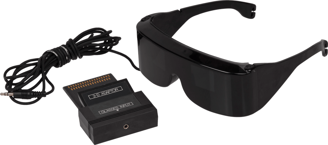
It turns out Sega also shipped ‘3D glasses’ as an official accessory! The glasses worked in sync with the CRT. During gameplay, the game alternates the position of objects between frames. Each lens contains an LCD screen that turns black to block your vision. The correct combination of graphics flickering and alternating shutters eventually creates a stereoscopic image in your head, resulting in a ‘3D’ effect.
The shutters are controlled via several memory addresses, but none of them indicate whether the glasses are actually plugged in. Therefore, games that support this accessory include a settings option to manually activate this feature.
The LCD controllers are interfaced with a jack cable, which plugs into the console. The European and American versions did not include the jack input, so they rely on the card port to connect an adaptor (we’ll see more about the card slot later on).
Video Output
The video-out connector of this system is incredibly versatile. It exposes both composite and RGB signals, which can be considered the two ‘extremes’ of video quality.
The downside, however, is that it doesn’t carry ‘composite sync’, so using the RGB output requires capturing the sync signal from composite, and its quality isn’t optimal.
Audio
The audio capabilities of this console are pretty much aligned with other 80s equipment. Inside the VDP chip, we find a slightly-customised version of the Texas Instruments SN76489 [11], which is a Programmable Sound Generator or ‘PSG’. This is the same type used in the NES/Famicom, albeit having different functions.
Functionality
A PSG can only synthesise a limited set of waveforms, with each channel allocated to a single waveform. I previously introduced some PSGs in the NES and the Game Boy article, if you are interested in this type of sound synthesis.
In the SMS, the PSG is programmed by altering its set of registers through the aforementioned I/O ports.
Let us now examine each type of waveform the SN76489 can synthesise:
Pulse
Pulse/Tone waves produce that iconic sound of the 8-bit generation. The sound wave is generated by latching up the voltage, holding it steady, and then dropping it. Repeating this at a constant rate produces a tone.
The period of the wave defines the frequency of the sound (musical note), while its duty cycle affects the timbre.
The SN76489, in particular, can produce three pulse waves at the same time. It also exposes a 10-bit counter on each channel that is used internally to latch the output, resulting in pulse waves with programmable frequencies.
Noise
Noise is a type of signal associated with interference. When outputted to a speaker, it sounds like static.
The SN76489 contains a Linear Feedback Shift Register (LFSR) which is fed with some input and cycled through to generate a pseudo-random signal. It can alternate between white noise and periodic noise.
The oscillator offers three frequencies to choose from, which alter the pitch of the noise [12]. There’s also a fourth option where the output of the third pulse channel modulates the noise channel. Some games used this option, combined with the periodic mode, to produce bass-like sounds (similar to a pulse at four octaves lower).
Overall, games typically use the noise channel for percussion or sound effects.
Mixed
So far we have discussed what each channel does individually. In practice, the TV receives a mono signal with all the channels mixed by the PSG.
Finally, the chip also contains programmable attenuators that lower the decibels of each channel, effectively acting as a volume control.
Secrets and limitations
Just like the VDP, the PSG is a no-brainer, but it does hide some interesting functionality:
FM Expansion
Double Dragon (1987).
The Japanese version of the Master System embedded an extra chip made by Yamaha called YM2413. It is drastically different from the PSG, as it uses frequency modulation to generate sound. I briefly explained how this works in the Mega Drive article, in case you are interested.
This chip adds nine audio channels. Each channel can either select one of the 16 preset instruments, or define a custom one by programming the carrier and modulator. Unfortunately, only one custom instrument is allowed at a time. On the other hand, the custom instrument offers interesting functions, such as ADSR envelope controls and feedback.
The YM2413 also has a second mode of operation called Rhythm mode, which instead provides six channels supplemented with five additional channels for rhythm instruments only.
The final sound output is generated by the YM2413, which mixes its channels with those of the PSG.
The Mark III variant did not include this chip, but FM functionality was available as an expansion unit called the FM Sound Unit. The European and American Master Systems, however, had to stick with the PSG, although some third-party modifications eventually appeared.
Emulation accuracy
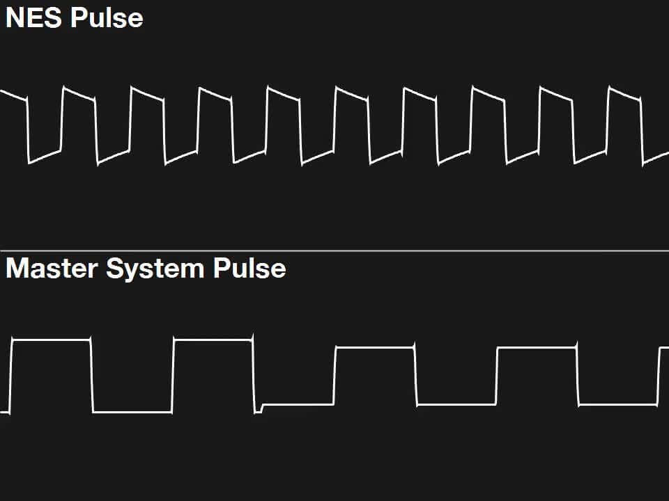
NES’ shows some decay while SGM’s is squared-shaped.
While reading through SMS Power (a website that collects extensive technical information about the system), I came across an interesting section called ‘The imperfect SN76489’ [13], which discusses some discrepancies I encountered while writing the article.
If you revisit the example video for the pulse wave, you will notice that it is visualised as an almost-perfect square wave. The pulse generator works by latching the voltage to generate the tone. However, in electrical circuits, components don’t just go from zero to one (or vice-versa) instantly; there is always a transient period, primarily due to the presence of filters in the electrical circuit.
Now, I use emulators to capture separate channels and avoid interference during recordings. Although, emulators do not always account for the transient factor, so their result may be closer to the ‘ideal scenario’ than the realistic behaviour found in 80s electronics. Take a look at the example image: both samples are taken from emulators, but the NES one potentially exhibits a behaviour closer to the analogue world.
I don’t have the necessary tools right now to confirm whether the SMS should exhibit similar behaviour. However, if it does, this does not imply that what you heard is incorrect - only that it may be at a slightly different volume, which is barely noticeable.
Sample play
While the SN76489 lacks a PCM channel for reproducing samples, there are some tricks that can be used to simulate this functionality.
These rely on the pulse channels, it was discovered that if the tone level is fixed at 1, the volume level (which alters the amplitude) conditions the shape of the waveform.
smspower.org describes various designs that enable the playback of 1-bit, 4-bit and 8-bit PCM samples. Although, storage requirements skyrocket with higher sample resolutions and rates, so these techniques are best exploited in homebrew games.
It is worth noting that streaming samples consumes a good amount of CPU cycles, and since there is only one processor in this system, the game may need to be halted for a short period.
I/O
Like other systems from its generation, the CPU is primarily responsible for handling I/O. In this case, the Z80 processor is unique for its specialised I/O addressing, but CPU cycles are still spent moving bits between components.
On the other side, the SMS uses a dedicated I/O controller chip to interface with the joypads and to enable or disable parts of the system, which alters the address map. Furthermore, this controller is essential for supporting the FM expansion, as the FM module exposes ports that conflict with the rest of the system.
Available interfaces
In addition to the two controller ports, the system contains one proprietary cartridge slot, one ‘Sega Card’ slot, and one expansion slot reserved for ‘future accessories’. The latter was never utilised, except for the FM expansion in the Mark III. Even so, the SMS and Mark III featured different expansion port designs [14].
Top interruptors
Another speciality about this console is the inclusion of two buttons on the top of its case: PAUSE and RESET. You can already guess what they do!
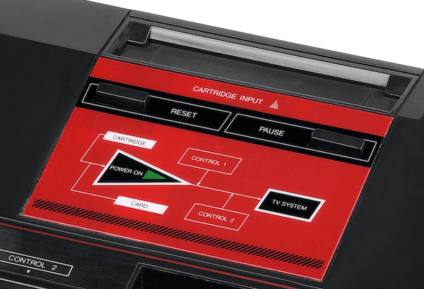
Pressing the PAUSE button sends a non-maskable interrupt to the CPU [16]. The interrupt handler is stored within the game itself, meaning it is up to the game to honour the press.
In contrast, and for some strange reason, the RESET button is handled as a keypress on the controller.
Operating System
There’s a small 8 KB BIOS ROM fitted on the motherboard that gets executed whenever the console is powered on. The program itself does not qualify as an ‘Operating System’; it is more accurately described as a Boot Manager.
Medium selector
The main goal of the BIOS is to bootstrap a valid game (from either game slot) in the following order of priority: the Sega Card, the cartridge, and the expansion module.
The boot process works as follows:
- The console is switched on.
- The BIOS copies part of its code to main RAM.
- This is a crucial step, since the program will start manipulating I/O ports, which will eventually disable access to the ROM!
- Show the splash screen (only in USA/Europe models).
- Check each slot for a valid game.
- This is done by talking to the I/O controller chip to activate the required slot. Then, the boot program copies the game header (16 bytes) from each slot to check if the game content is valid (thus, properly inserted). The header must have
TMR SEGAencoded.
- This is done by talking to the I/O controller chip to activate the required slot. Then, the boot program copies the game header (16 bytes) from each slot to check if the game content is valid (thus, properly inserted). The header must have
- Perform the region check.
- Redirect execution to the game.
Surprise screen
If any of the checks fail, the console loops indefinitely while showing a screen that prompts the user to insert a valid game.
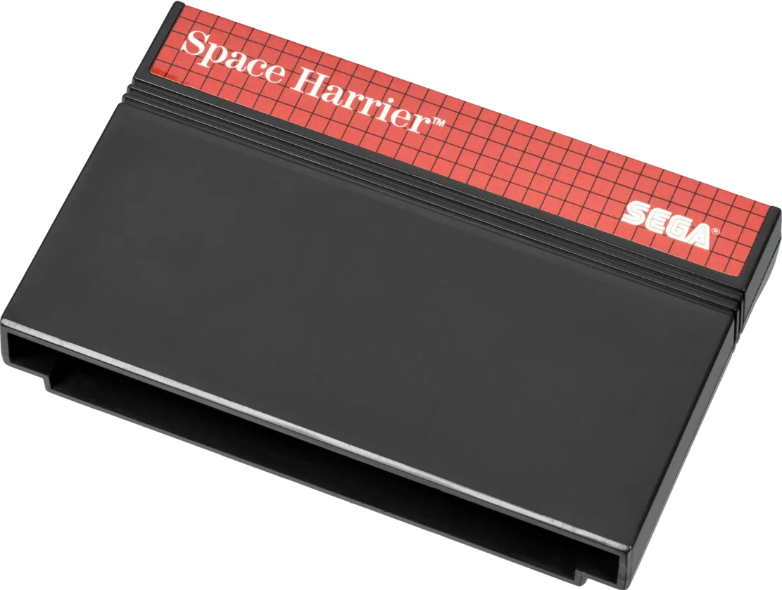
I have to say, in terms of the design of the error screen, the creative differences between regions are quite significant. The first time I heard the colourful Japanese version, I thought it was based on Electric Light Orchestra (the band), but it is actually from Space Harrier (the game). Also, the perspective effect on the floor is accomplished by altering the colour palettes.
More regional differences
Because the Japanese variant was backwards compatible with the SG-1000, the header check is replaced with an ‘integrity check’ that instead reads data from the first 256 bytes multiple times to detect if it is garbage.
Furthermore, the Mark III doesn’t have a BIOS, so the slots are activated with hardware switches. Furthermore, the cartridge is the medium with the most priority.
Updatability and later BIOS chips
The BIOS ROM, by its nature, is not updatable. Although, as new console revisions entered the market, it was discovered that Sega also updated the BIOS program.
Later ROMs even embedded entire games! As a consequence, the chip got bigger and was accompanied by a dedicated mapper.
Games
To make a long story short, games were written in plain Z80 assembly, that’s it. There were no compilers or high-level tools back then, apart from the assembler.
Medium
The Master System supports two different media for distributing games:
- The Cartridge: The most common one, capable of addressing up to 48 KB of memory. However, by including a mapper, the system could access a wider range and handle additional chips, such as battery-backed RAM for storing saves.
- Sega offered to developers official mappers called ‘Paging Chips’. The most powerful one could map up to 512 KB of memory.
- The Sega Card: Visibly thinner and cheaper to manufacture, but it could only access up to 32 KB of memory. Since SEGA never designed a mapper for this medium, the largest card found on the market contained a 32 KB ROM.
Anti-Piracy and Region locking
Unlike Nintendo, Sega did not employ aggressive methods to control the distribution of their games. They did, however, prevent American and European systems from running Japanese games by altering the shape of the cartridge slot and implementing a different ROM header check.
Furthermore, American and European systems were required to include the aforementioned TMR SEGA code in their header. I suppose this enabled them to prevent unauthorised distribution by leveraging trademark laws.
That’s all folks
Having previously written the Nintendo DS article really puts into perspective how complicated technology has become. The Master System is very straightforward by comparison, even after some ‘technical nitpicking’ I may have expressed here and there.
Anyway, I hope this article provided you with a comprehensive overview of the state of technology of the early-to-mid-80s. I also want to thank the smspower.org community and the /r/Emulation discord for reading the first draft and pointing out lots of corrections and suggestions.
Until next time!
Rodrigo
Dedicated to the memory of Jacinto ‘Pocho’ Fornasier.