Supporting imagery
Models
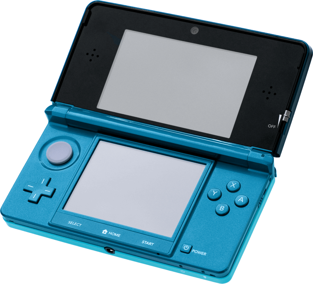
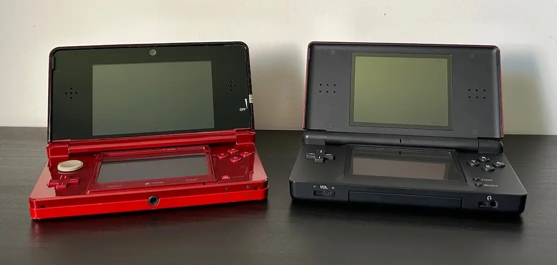
Released on 26/02/2011 in Japan, 25/03/2011 in Europe and 27/03/2011 in America.
Motherboard
Diagram
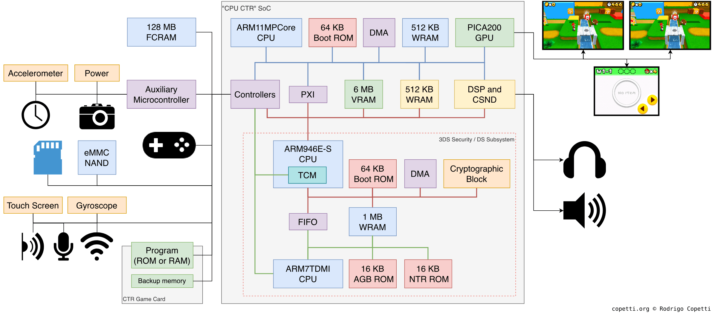
Even as complex as it is, I had to leave out the old DS and GBA A/V subsystem.
A quick introduction
As smartphones surge in adoption, the videogame market is experiencing an unusual growth led by discount App Stores and affordable development licences. With this, one can only wonder when kids will prefer an iPhone 4 over a Nintendo DSi.
In the midst of finding out the answer, Nintendo conceives a thrilling successor to its triumphant portable system. In it, users will find old, present and unfamiliar technology - many of which can’t be replicated by smartphones.
And so, this new production of the Architecture of Consoles series will give you a profound description of how this new console works, both internally and externally.
Recommended reading
If you are new to this article series, I strongly suggest reading the GameCube, Game Boy Advance and Nintendo DS articles beforehand, as they will explain various terms and concepts referenced in this one.
Models and variants
Throughout the lifecycle (and struggles) of this console, Nintendo released numerous revisions in an attempt to correct its target audience and recover loyal customers.
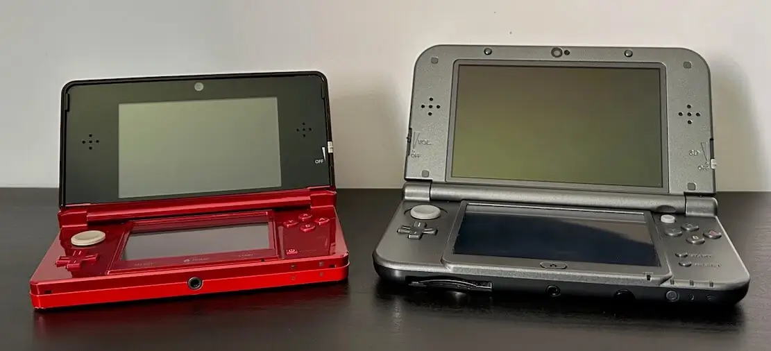
From the architectural point of view, there were a total of six different models:
- Nintendo 3DS (2011) and Nintendo 3DS XL (2012): The debuting series featuring the original architecture. The only relevant difference between the XL and non-XL models is the screen size.
- Nintendo 2DS (2013): A cheaper alternative to the original Nintendo 3DS by removing the stereoscopic screen and featuring a Game Boy-inspired shape.
- New Nintendo 3DS (2014) and New Nintendo 3DS XL (2015): A re-engineering of the standard 3DS models. The ‘New’ variants exhibit an incremental hardware upgrade, an NFC reader, a larger button set and an improved stereoscopic system.
- New Nintendo 2DS XL (2017): The ‘New’ affordable alternative to the New Nintendo 3DS XL by omitting stereoscopic functionality.
Now, for this article, the focus will be on the original Nintendo 3DS (after all, it’s the lowest common denominator for games). However, since the architectural differences of the ‘New’ series are worth studying, these will receive a dedicated section.
Displays
There’s only one company that keeps altering the standard structure of all my analyses, and that’s Nintendo. This time, I need to start with the stereoscopic screens (a.k.a. ‘3D without glasses’) before diving into anything else.
First things first, the Nintendo 3DS, as a successor of the Nintendo DS, includes two LCD screens. The upper screen has a resolution of 800 x 240 pixels and somehow can display images with a sense of depth. When I first read this, only questions popped into my head:
- What optics principles are they applying?
- How is the screen designed?
- How do games comply with this system?
Well, here are the answers!
Principles
Liked it or not, the fundamentals are not so different from the Virtual Boy, which I’ve happened to analyse two years before. To recall, the Virtual Boy displays two images, one to each eye, and shows objects individually shifted from the centre. By looking at the two pictures at the same time, they are perceived as some objects are behind others (sense of depth). This is the basis of Stereoscopic Parallax.
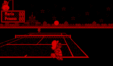
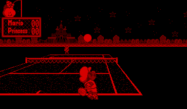
Mario’s Tennis (1995).
Now, the way the Virtual Boy executed this was a bit cumbersome: it required users to place their heads close to the eyepiece and then adjust the focal length and inter-pupil distance. 15 years later, Nintendo rightly said ‘No’ to all of that nuisance, and designed a new system where users could enjoy 3D-looking scenery without considerable intervention.
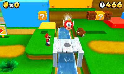
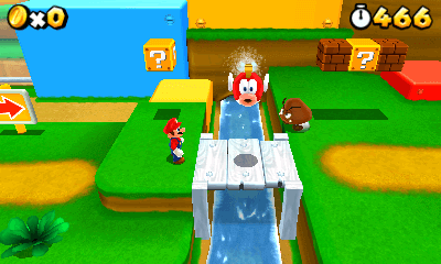
Super Mario 3D Land (2011).
This brings us to our next question.
The special screen
Take a look again at the resolution of the upper LCD screen. On paper, it says it’s 800 x 240 pixels wide, which results in a ludicrous aspect ratio.

In reality, the physical screen is made of half-width pixels and operates in two modes:
- Traditional/2D mode: When the stereoscopic function is disabled, groups of two horizontal pixel pairs are treated as a single one.
- To tell the truth, the screen can still display a frame of 800 x 240 px, although no commercial game ever used this.
- Stereoscopic/3D mode: All pixels are treated individually, and with it, the screen displays two frames of 400 x 240 pixels at the same time.
Moreover, to perform stereoscopic parallax, this particular LCD houses an extra layer called Parallax Barrier [2]. These opaque shutters deviate the backlight beamed behind the pixels of the LCD, so each eye will receive the light of a different subset of pixels [3]. The half-width pixels will also appear to be wider, thereby giving the feeling they have the traditional aspect ratio.
All in all, this recreates the original effect of the Virtual Boy without requiring controls for adjustment.
The technology is not perfect, however, as there are a few caveats:
- The parallax barrier requires extra brightness, thereby impacting the battery life.
- The user must not hold the screen in a tilted position (compared to the user’s eyes). Otherwise, the user will end up seeing a confusing mix of the two parallax frames, which can be a disorienting experience. Not to mention the eyes won’t enjoy the extra fatigue.
- Combining the fact that the user must maintain a fixed posture while playing, and that stereoscopic parallax can tire the eyes quicker. The 3D feature, as a whole, can easily become an unnecessary hassle for most.
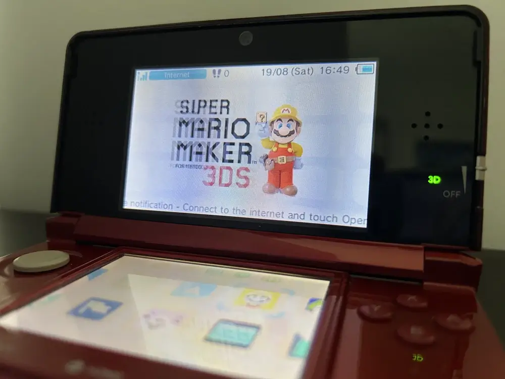
To remediate things, Nintendo added a slider control (called 3D depth slider) to adjust the level of depth between objects. In doing so, it either increases or decreases the difference between the two frames. This was done to reduce the depth effect for people who didn’t find it enjoyable or too fatiguing.
Setting the 3D slider to the max can be disorienting at first. In my experience, my eyes eventually got focused, at which point I perceived the top LCD screen as if I were looking through a window. The main problem is that users will need to continuously shift their eyes to see the bottom screen, and the repeated action can be very straining.
As a side note, one can’t help but find it amusing how the graphics pipeline has gone full circle when rendering stereoscopic frames. During rendering, 3D data is projected into a 2D space, and now with the stereoscopic screen, the third dimension is ‘restored’. At this point, let’s just use holograms and skip the 3D projection stage altogether!
A small update

With the advent of the ‘New 3DS’ model, Nintendo revisioned their stereoscopic screen in an effort to reach enjoyability levels. In the new model, the console incorporates a face-tracking mechanism to tackle the tilting effect, so users don’t need to worry about keeping a good ‘head-console posture’ anymore.
The special games
Now for this system to work, games must play along (pun intended). Just like they traditionally interact with the GPU to draw frames on the display, they must now broadcast two frames of the scenery but with objects slightly shifted.
To make life easier for developers, there are official APIs that assist in this, especially for those games with 3D sceneries. These APIs help by providing routines that construct two projection matrices, the graphics pipeline then uses them to render the two slightly-shifted frames.
CPU
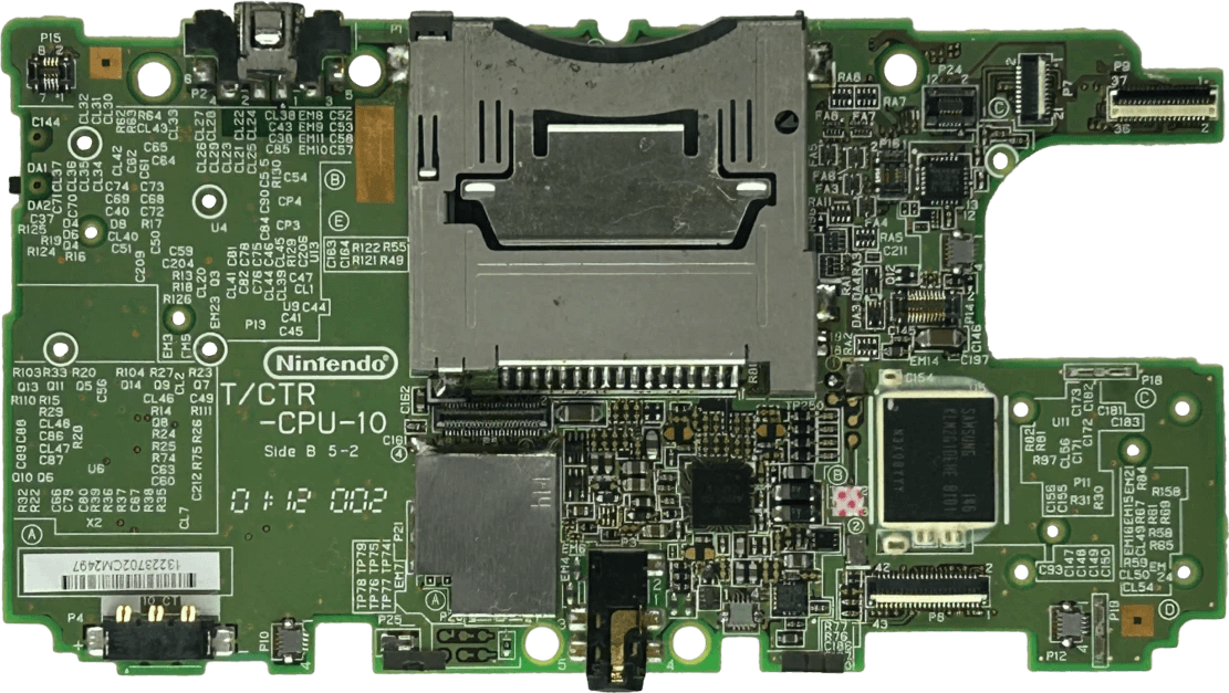
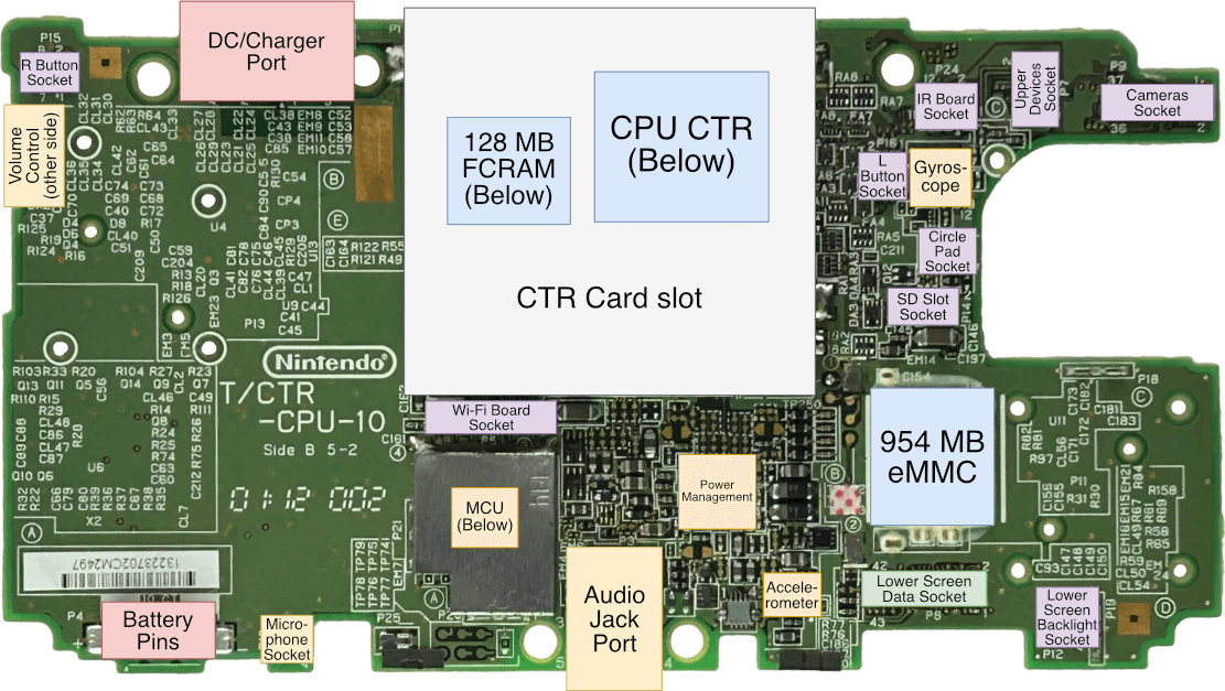
Now that we know how the display works, let’s look at the internals of this console. If you get a hold of the motherboard, you’ll see three big chips, one being the CPU CTR. That’s the big System-On-Chip (SoC) that houses the entire system (aside from storage and RAM).
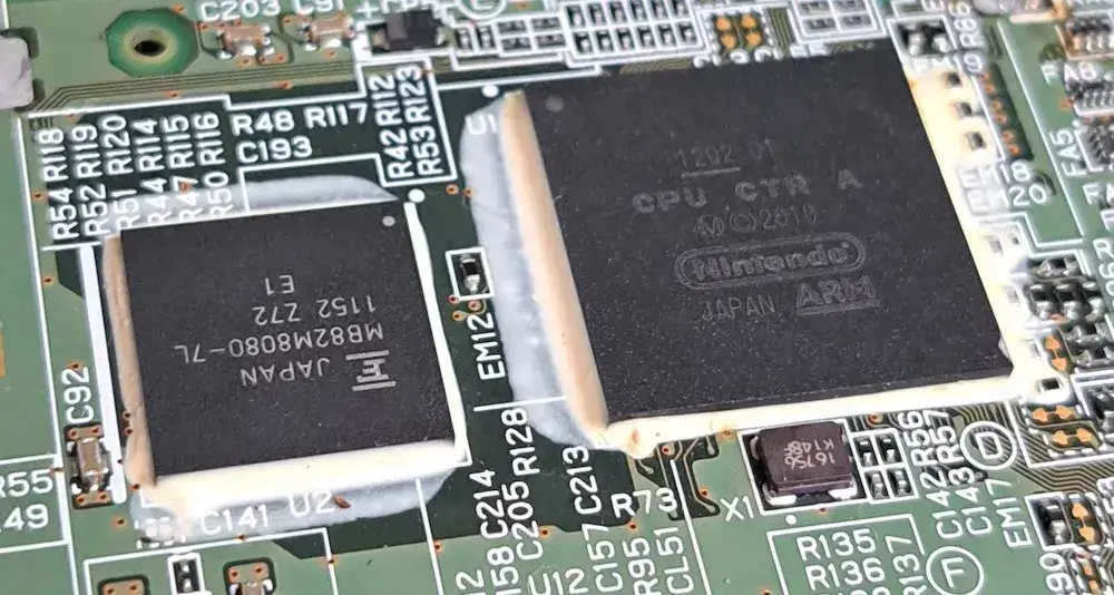
CPU CTR follows the design methods of previous portable consoles from Nintendo. That is, squash all your engineering into a single block. In doing so, it will reduce the production of counterfeits, protect sensible components and improve heat dissipation.
In terms of the actual CPU, Nintendo partnered again with their old friend, ARM, to produce their next-generation core. ARM’s traditional licensing model (based on offering synthesisable designs) allows Nintendo to mould a CPU to their needs, including fitting it into a big and opaque SoC. In the end, ARM gave them a relatively antiquated product with substantial upgrades. Their choice was the ARM11, a successor of the ARM9 (featured in the Nintendo DS). More specifically, the MPCore variant, ARM’s first homogenous multi-core solution.
Using ARM’s designs, Nintendo crafted an ARM11 MPCore cluster housing two ARM11 cores [4]. Three years later, with the arrival of the ‘New’ 3DS, the SoC was expanded to contain four ARM11 cores. The effects of this will be explained in due time. So, before anything else, let’s analyse what the new CPU cores offer to this console.
An iconic industry
The ARM11 series originated in 2002. By then, cellphones ran Java ME applications and bragged about ringtones with actual melodies. In the coming years, the ARM11 became a flagship in the mobile CPU sector, displacing the popular ARM9, the short-lived ARM10 and Intel’s XScale. The latter was the continuation of StrongARM, which Intel later sold off to focus on ‘low-power’ x86 CPUs… if only they knew that the mobile market would skyrocket!
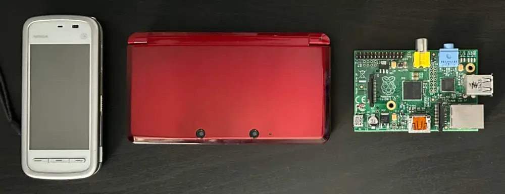
In the end, ARM11s became known for powering the 2006-2009 generation of smartphones. This generation featured a mix of keypad, clamshell and full touchscreen designs. If you owned a Nokia N95, 5230 or the first iPhone, you’ve used an ARM11. This also applied to many high-end cameras, GPS or similar peripherals. Curiously enough, other manufacturers like RIM and Samsung held onto the Intel XScale until 2009. On a side note, the ARM11 was also the choice of CPU for the first Raspberry Pi.
Now, by the time Nintendo adopted the ARM11, its creator had already succeeded it with the Cortex-A series. This is nothing but expected, as Nintendo’s model favours cost-effectiveness over avant-garde CPUs. Look at it from another way, saving in CPU costs allows them to focus their budget on other aspects of the console, you’ll soon see.
New dialects…
Along with the new shiny CPUs, a new instruction set arrived, the ARMv6.
From a programmer’s perspective, the ARMv6 ISA innovates with a new set of vector instructions and multi-core support [5]. The new vector set is made of SIMD instructions that operate groups of four 8-bit values or two 16-bit values at a time (using the existing 32-bit registers) [6]. These instructions can only operate integers (no floating point), however. Moving on, the new multi-core instructions consist of ‘store’ and ‘load’ opcodes with special care for synchronisation (this is crucial when multiple CPUs use the same memory locations) [7].
All in all, this may not seem that thriving for a new chip series, but remember that ARM’s CPUs speak many ‘languages’. In the case of an ARM11-based core, you are provided with:
- The main 32-bit ISA, called ARMv6.
- A compressed alternative called Thumb. Its instructions fit in 16-bit words instead. If you’d like to know more, I go over it in the Game Boy Advance and Nintendo DS articles, as it weighs significant importance in those consoles.
- Jazelle, a Java bytecode interpreter, though mostly forgotten and left unused. I’ve mentioned a bit of it in the Wii article.
- Any extension bundled into the core. For instance, the MPCore includes a Vector Floating-point Coprocessor (VFP) with additional instructions to control said coprocessor [8]. I talk more about this later.
To make matters less confusing, ARM tends to package all of these with a single nomenclature. For instance, in the case of the ARM11 MPCore opcodes, ARM refers to this variant as the ARMv6k instruction set.
… and a fragmented distribution
Be as it may, the adoption of extensions and alternative instruction sets eventually made things very convoluted for developers targeting generic ARM hardware, you only have to look at the uncountable ARM ports devised for Linux distributions.
Debian, one of the most popular distributions, tried to tackle the disparities by developing two ports in parallel:
armel: For wide compatibility (ARMv4T and onwards).armhf: Accelerated with the VFP extension, but only compatible with ARMv7 onwards.
Yet, with the arrival of the Raspberry Pi (powered by ARMv6 and accelerated with the VFP), neither of them was deemed acceptable. Thus, an unofficial port called ‘Raspbian’ was developed to provide a VFP-accelerated version for ARMv6 CPUs [9]. Even so, the trend continued: years later, with the arrival of ARMv8 and AArch64, Debian spawned yet-another port, arm64, optimised for the new 64-bits ISA.
I don’t remember seeing this labyrinth with x86 (even though the adoption of x86 SIMD extensions hasn’t been consistent, to say the least), but at least things are now getting more orderly. AArch64 has unified many extensions and dropped alternative modes (farewell, Thumb and Jazelle).
Core functionality
… That was a quick detour, let’s go back to analysing what’s in the 3DS CPU!
For this study, we can divide the ARM11 MPCore into two areas:
- The MP11 cores that make up the cluster.
- The Advanced eXtensible Interface (AXI) bus, a new invention that interconnects the cores and interfaces with the outside world.
Let’s start with the cores now and then we’ll check the AXI bus.
The original MPCore
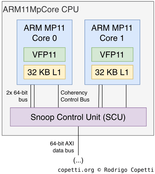
The first ARM11 MPCore variant, which debuted with the original 3DS, includes two cores. Each is called MP11 and runs at 268 MHz [10].
Apart from implementing the ARMv6k instruction set, the MP11 features an 8-stage pipeline [11] and it’s complemented with two levels of branch prediction: ‘dynamic’ (based on previous executions) and ‘static’ (based on the current instruction alone). Overall, I sense these new additions are part of a new design philosophy that will eventually obsolete the iconic conditional execution, although we won’t notice this until the next generation.
Additionally, since the ARM946E-S CPU, ARM has been fitting a System Control Coprocessor called CP15. This time, it provides Memory-Management (MMU functions) and register memory that output information about the MPCore cluster.
Now, there’s no more Tightly-Coupled Memory (TCM). There are however 16 KB of instruction cache and 16 KB of data cache, this change of model resembles other systems of the same generation. If you are curious, this L1 cache is 4-way set associative.
Finally, each core houses a co-processor called Vector Floating-point Coprocessor (also known as ‘VFP’, or ‘VFP11’ in the case of the ARM11). This accelerates arithmetic operations with floating-point numbers, both 32-bit single-precision (a.k.a. float) and 64-bit double-precision (a.k.a. double) ones [12]. It’s not a big coprocessor though, as its register file is composed of thirty-two 32-bit registers, so doubles will consume two registers. In any case, this processor implements the VFPv2 instruction set and follows the IEEE 754 standard. The latter is a welcomed decision, considering the difficulties of previous generations.
The ‘New’ MPCore
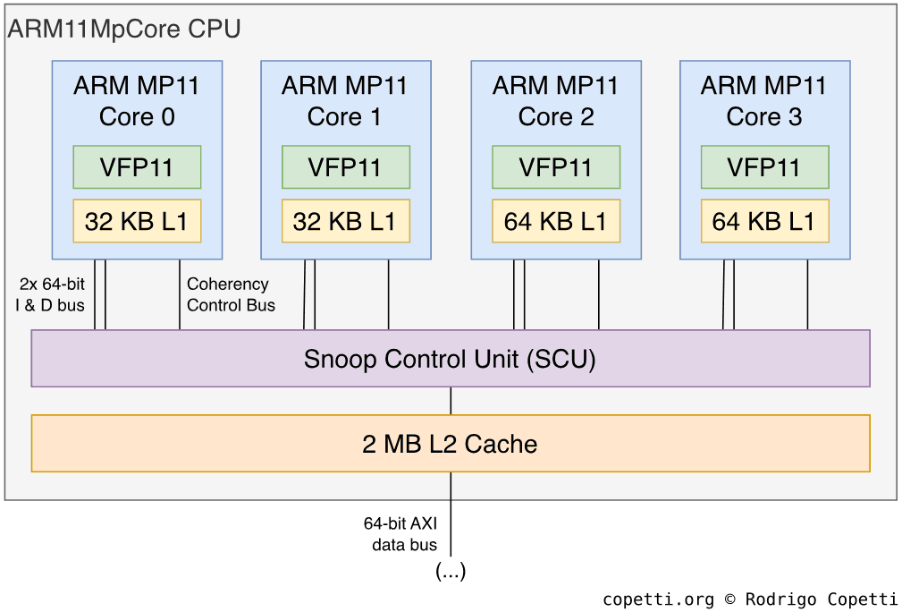
With the arrival of the New 3DS in 2014, a new SoC was included (CPU LGR) and with it, a luxurious CPU upgrade.
The most apparent change is that we have now four MP11 cores instead of two. The consequences of this, however, are not simple to disseminate, but we’ll see them in due time.
The second change is that the CPU incorporates 2 MB of L2 cache shared between the four cores. This type of cache is 16-way associative, which anticipates four cores accessing it at the same time. If you’d like to know more, I went over associative caches with the Xbox 360 article.
Moving on, all cores now run at 804 MHz (three times the original speed, which will certainly raise a few eyebrows).
The AXI bus
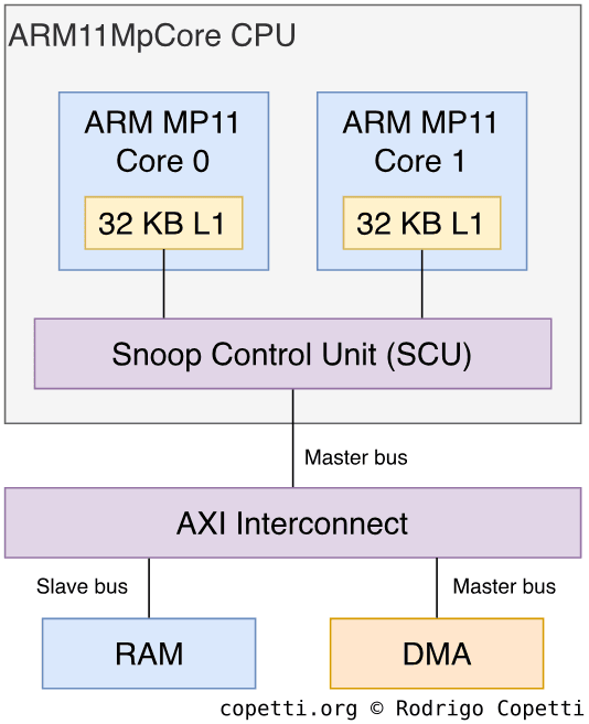
Whether we’re talking about two or four MP11 cores, all of these are connected using a popular bus, proudly authored by ARM, called the Advanced eXtensible Interface (AXI). This protocol is part of the AMBA3 model, a successor of the original AMBA revision that we’ve seen in the Wii and Wii U (both housing an ARM9 CPU). In doing so, ARM offered the AXI model as a critical building block for System On Chips (SoC).
Generally speaking, the AXI model provides a set of protocols for connecting components with distinct bandwidth requirements. These are free to choose any particular topology, like the token-ring model of the PlayStation 3 or the mesh solution made for the Xbox 360. Now, within the Nintendo 3DS, we find a combination of bus and star designs.
Following AMBA’s methodologies for interconnecting nodes, there will be a master-slave hierarchy to denote which entity is in charge. The master components (typically, the CPU cores) will be the ones sending commands to the slaves (i.e. memory and I/O blocks).
Furthermore, the AXI network can be arbitrated using a dedicated block (called AXI interconnect) acting as a bus matrix [13]. This is what we find in the MPCore and relies on individual 64-bit buses [14]. In doing so, the network tackles the congestion of high-bandwidth components (something that consoles like the PlayStation 2 struggled with). Moreover, multiple master devices can communicate with slave nodes using separate channels to avoid waiting for other masters to finish. And if that’s not enough, traditional enhancements like burst transactions are also implemented, from which the MP11 cores take advantage.
In the case of the 3DS, the AXI interconnect is housed in a bigger block called Snoop Control Unit (SCU) that also takes care of automatically maintaining L1 cache coherency between the MP11 cores.
Any other CPUs?
Up to this moment, I’ve been talking about the MPCore as if it were the only CPU in this system, the reason being mixing up distinct CPUs for this analysis can turn it into an incomprehensible essay. That is, until now.
The truth is, Nintendo had extra requirements for this console. They wanted a proper security system, but also the possibility to turn the console into a Nintendo DSi or a GBA on-the-fly. So, for all of that, they ended up bundling three distinct CPU packages - one being the mentioned ARM11. The other two are well hidden, in the sense that games are completely unaware of them. In fact, 3DS emulators like Citra don’t care about them at all [15].
But we do! So here’s the complete list of the CPUs this system houses:
- The ARM11 MPCore we’ve just seen.
- An ARM946E-S from the Nintendo DS days. It’s treated as a secret co-processor and it’s only managed by the operating system. Alternatively, it becomes the main processor whenever a DS or DSi game is executed.
- Thanks to its bundled CP15 co-processor, there’s a Memory Protection Unit (MPU) in place. This will protect the CPU from arbitrarily executing code from any location in memory.
- An ARM7TDMI from the Game Boy Advance days. It’s a relatively ignored CPU, unless a DS or DSi game is being played, in which case it acts as a co-processor. However, on the special occasion when a Game Boy Advanced game is running, the main execution falls into this CPU.
Unfortunately, or for obvious reasons, the three CPUs are never usable at the same time. Instead, the console has three modes of operation:
- Native 3DS mode: The ARM11 MPCore executes a 3DS game while the ARM946E-S deals with I/O and security. The ARM7, on the other side, is switched off.
- Nintendo DSi mode: The ARM946E-S and ARM7TDMI operate in a multi-processor configuration to execute a Nintendo DS or DSi game. Just like with its predecessor, the ARM7TDMI has greater access to I/O. Meanwhile, the ARM11 MPCore will be working in the background to replicate missing and re-located DS hardware (real-time clock, power management, keypad, GBA/DS PPU display and so forth).
- Game Boy Advance mode: The ARM7TDMI is the only CPU executing instructions (in 99% of cases, that will come from a GBA game). The ARM11 MPCore and ARM9, both still operating within the capacities of ‘Native 3DS mode’, will be working in the background.
If you stop to think about it, the Nintendo 3DS ends up housing four processors in total (Two MP11 cores + one ARM9 + one ARM7), or the absurd amount of six in the case of the New 3DS. How convoluted is that? Luckily, this system didn’t suffer the complications of the Sega Saturn and you can thank Nintendo and ARM’s engineering for that. After all, 3DS developers only had to deal with the MPCore.
Since the ARM9 and ARM7 are predominantly for I/O, security and backwards compatibility (neither of which require the developer’s awareness), I discuss them in later sections of this article. But if you’d like to know more about the design of the ARM7 and ARM9, I wrote about them in previous articles (the Game Boy Advance and Nintendo DS ones, respectively).
Multi-core communication
I guess the question now is, how can CPUs and cores talk to each other? Well, the easiest way is to share RAM… but you could also try a more efficient approach, depending on the cores trying to communicate:

- With inter-core ARM11 communication, a core can send interrupts to another core by writing on its
Software Interrupt Register[16]. - In the case of ARM11↔︎ARM9 or ARM9↔︎ARM7 communication, the same FIFO model from the Nintendo DS is implemented. Plus, the ARM11↔︎ARM9 FIFO is also called ‘PXI’ [17].
Memory available
Having three different CPUs also means the memory layout will not be simple, especially if you care about security.
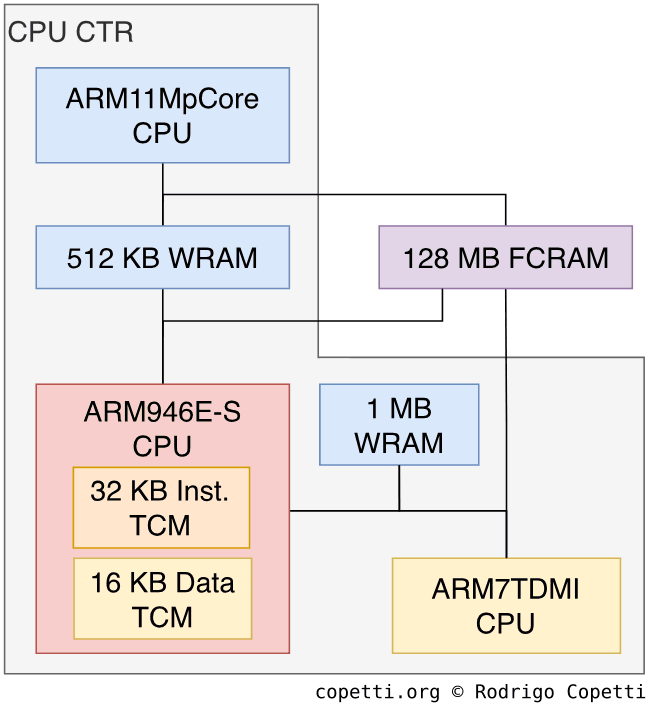
To make a long story short, we’ve got the following blocks:
- From the developer’s perspective, the system provides 128 MB of FCRAM. The New 3DS increased this to 256 MB. The rest is redundant for games.
- For predominantly security reasons, the ARM11 is also provided with a fast block of 512 KB of SRAM. The ARM9 is also given a block of 1 MB of SRAM (1.5 MB in the case of the New 3DS).
- By inheriting the model of the Nintendo DS, the ARM9 also houses Tightly-Coupled Memory (TCM). Particularly, there’s 32 KB for instructions and 16 KB for data.
A new type of memory spotted
It’s all jolly that the Nintendo 3DS includes 32 times the general-purpose memory of its predecessor, but what’s that ‘FCRAM’? Is it any different from the other standards?
Well, Fast Cycle DRAM (FCRAM) is yet another RAM invention, this time authored in 2002 by Fujitsu and Toshiba. Presented as an alternative to DRAM-based technology (i.e. SDRAM, EDO DRAM, RDRAM, etc.), FCRAM excels on non-continuous reads, where it exhibits a lower latency than DRAM [18]. This was done to replicate the performance offered by the more expensive SRAM.
FCRAM competes directly with DDR DRAM by offering a revamped design of the memory arrays. In place of adding more circuitry on top of it, arrays are split into smaller subblocks, which are then accessed using a 3-stage pipeline [19]. In doing so, reading and writing on random locations become faster. These changes are still designed with backwards compatibility in mind. Thus, FCRAM is compatible with DDR DRAM controllers (hence, its full name is ‘DDR FCRAM’).
Faster memory transfers
The inventors of the MPCore and the AMBA bus happen to also offer a brand of DMA controllers called CoreLink, with Nintendo being a loyal client. So, it’s no mystery as to why the 3DS bundles multiple blocks of CoreLink DMA-330 into their SoC [20].
These DMAs in particular are attached to an AXI bus and act as master devices. Each can transfer data between two slaves interconnected with the AMBA protocol (either AXI or the slower APB) [21].
Nintendo fitted one CoreLink DMA next to the ARM9, this is referred to as XDMA and provides up to four channels (thus, up to four concurrent transfers). There’s another DMA next to the ARM11 block, this time called CDMA, which provides up to eight channels. With the arrival of the New 3DS, another CoreLink DMA-330 is fitted next to the ARM11 block (now a quad-core cluster).
Programming
With all being said, how do you program a system featuring this unorthodox CPU arrangement? To be fair, unusual systems are no strangers to videogame developers. But in this case, 3DS programmers only have access to the ARM11 MPCore. Furthermore, once you reach the ‘Operating System’ section, you’ll learn the abilities with this cluster are further restricted.
In any case, no matter the console revision, programmers base their algorithms on the multi-threading model: the program groups sequences of instructions using threads, these are then dispatched by the operating system to the physical cores, as the former deems fit. Once a novelty for Xbox 360 software, this standard provides a layer of abstraction that blinds the developers from writing software only compatible with a fixed number and type of CPU cores.
Dealing with the ‘New’ hardware
Since the New 3DS diverts considerably from the original specification, Nintendo set up a thin compatibility layer to enable old 3DS games to work with the new hardware without manual intervention.
In essence, when a game is launched from a New 3DS console, the game’s code specifies if it’s specifically targeting the new models or not [22]. If it is, the operating system will proceed to activate all the novelties (faster clock speed, extra RAM and use of L2 cache) for that game to enjoy. If it’s not, the operating system will keep its exclusive hardware deactivated until the user exits the game, so the game can safely assume it’s running on the old hardware and will do so without issue.
To keep supporting the old 3DS, games can be packaged with two codebases (one for the ‘New’ model and the other for the ‘Old’ one). It’s up to the game studios to decide whether to support the old and new 3DS, or only the new 3DS.
You may be wondering what happens with the rest of the exclusive hardware the New 3DS houses (i.e. extra ARM11 cores and DMA). Well, to properly understand the rationale, I explain this once you reach the ‘Operating System’ section, but I’m afraid you won’t like the answer!
Graphics
Next to a new CPU is always a modern GPU. So, what kind of Picture Processing Unit did Nintendo build this time? To tell the truth, none. For the first time in their portable line, they resorted to a GPU vendor.
Nevertheless, the requirements of Nintendo haven’t shifted. The company still wanted a chip with acceptable performance… and the intellectual property core. This will allow them to embed the GPU into their SoC, in the same way they did with the ARM CPUs.
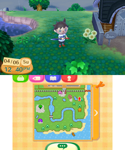
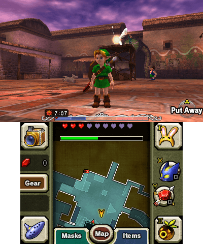
Meanwhile, a potential candidate just finished unveiling their new invention at SIGGRAPH 2006 [23]. For some time, Digital Media Professionals Inc. (also known as ‘DMP’) have been building affordable GPUs for the embedded market and, while their chips are nothing out of the ordinary, they guarantee decent OpenGL ES support. Furthermore, their licensing framework offers synthesisable GPUs.
This seemed enough for Nintendo, who happily negotiated a license for DMP’s latest core, the PICA200 and subsequently bundled it inside CPU CTR (the Nintendo 3DS’ SoC). The GPU runs at 268 MHz.
Architecture of the PICA200
If I had to summarise it in one sentence, the PICA200 is a budget low-power 3D processor that combines a pre-unified architecture with a modernised API. The underlying architecture of the PICA200 is called Maestro 2G [24] and its design is compliant with OpenGL ES 1.1, but extended with elements from OpenGL ES 2.0 [25]. However, the PICA200’s APIs are not limited to either standard.
You see, even though the pipeline is segregated and the pixel stage is fixed-function (à la PlayStation 2), DMP expanded the limited circuitry with a set of Maestro functions that provide capabilities beyond the expectations of the embedded market [26]. This includes fragment lighting, multiple shadowing algorithms, polygon subdivision, bump mapping, procedural textures and many fog effects.
Additionally and in contrast to the Nintendo DS, the PICA200 only works with framebuffers. That’s it. The sprite engine, a popular workaround to tackle unaffordable memory requirements, is now a thing of the past. This also includes scan-line tricks, as contemporary GPUs work way faster than the refresh rate of a CRT.
Organising the content
Now that we know that this console can draw 3D shapes, the question now is: where does it store its materials? There are two locations, the large FCRAM block and the smaller but faster VRAM.
Nintendo only provided 6 MB of VRAM exclusively for the GPU. Ideally, programmers would fit as much as they can there, but since it will fill up pretty quickly, it is expected to be used to store data that needs instant access (i.e. commands, buffers and recurrent textures) while placing the rest on FCRAM. The PICA200 comes with a DMA unit that can transfer data between FCRAM and VRAM. So, at the end of the day, it’s the responsibility of the programmer to come up with an efficient placement to avoid bottlenecks.
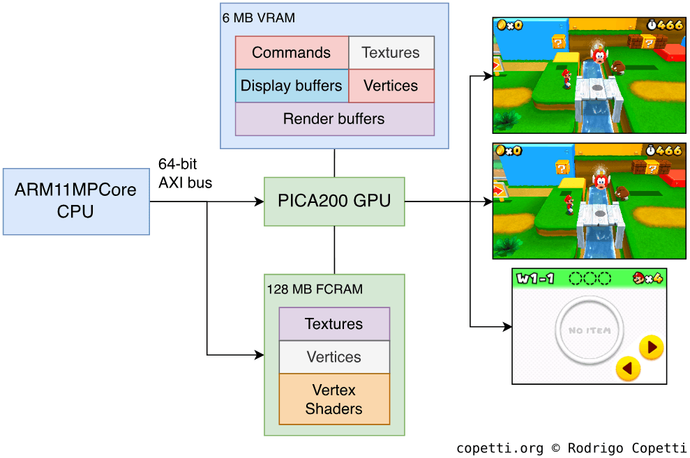
During rendering, programmers allocate dedicated render buffers (i.e. frame, stencil, depth, etc.) for many operations. That’s always been the case. With the 3DS, however, the LCD controllers don’t understand the data that the PICA200 renders in the frame-buffer. Thus, programmers are also expected to reserve extra space for LCD frame-buffers [27]. Each is bound to a physical screen and encodes the frame in the required format for the LCD controller.
This means that the 3DS is required to allocate at least three LCD frame-buffers (two for the stereoscopic upper screen and one for the bottom one). However, to avoid showing artefacts, a duplicate set may be allocated to perform page flipping.
Based on this, the display process works as follows:
- The LCD continuously displays the content of the active LCD frame-buffer, as instructed by an index register.
- Meanwhile, the GPU finishes rendering new geometry in a separate frame-buffer.
- The frame-buffer is exported to the inactive LCD frame-buffer.
- The GPU swaps the index of the active LCD frame-buffer.
- For practical reasons, the index swap happens at the end of Vertical Sync to avoid tearing down the picture [28].
- The LCD will now be scanning the recently updated LCD frame-buffer from now on.
Adopting open standards
On an interesting note, just like the ARM11 MPCore adopts ARM’s AXI protocol for interconnecting its cores, DMP adopted a less-proprietary option called Open Core Protocol (OCP) [29]. As its name indicates, the Open Core protocol does not impose any licensing restrictions on its users, something that vendors using the PICA200 may find advantageous. For comparison purposes, AXI was released in 2003 (along with the AMBA 3 specification) while OCP was published in 2001. It does make me wonder what kind of technology Nintendo fitted to adapt the OCP signal coming from the PICA200 into an AXI-compliant signal, so the rest of the SoC understands it. I assume that there’s a bridge between the PICA200 and the AXI bus.
Interestingly enough, the predecessor of the PICA200, the ULTRAY2000, shares many similarities with its successor. The most notable difference, however, is that the data interfaces use the PCI and DDR-SDRAM protocols instead [30].
Constructing the frame
Naturally, the GPU is not aware of the stereoscopic or dual-screen nature of the displays, it will only be tasked with rendering three screens during gameplay:
- Top stereoscopic-left: 400 x 240 pixels wide.
- Top stereoscopic-right: 400 x 240 pixels wide.
- Bottom: 320 x 240 pixels wide.
All of them can display 8-bit RGB colours, which equates to up to 16.78 million colours.
Considering players will expect acceptable frame rates on all three screens (especially on the first two), the single PICA200 will be subject to high amounts of workload throughout its operation, an important aspect to remember when judging its performance.
That being said, here is an overview of how data travels to draw a single frame:
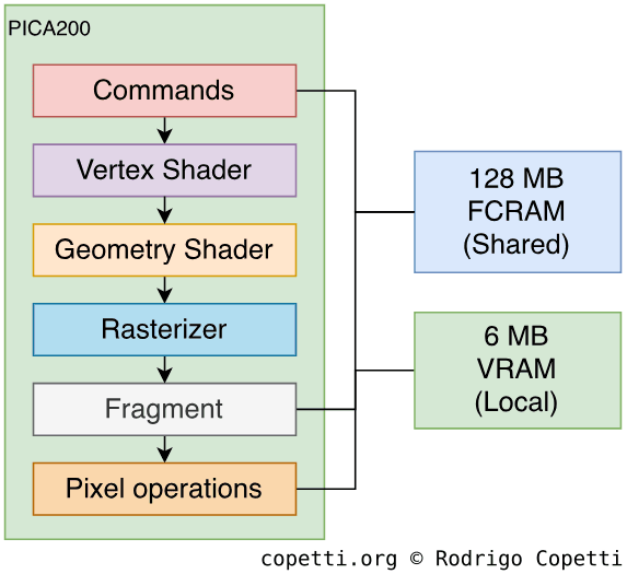
… and as customary in this series of articles, we’ll now take a look at what happens at each stage.
Commands
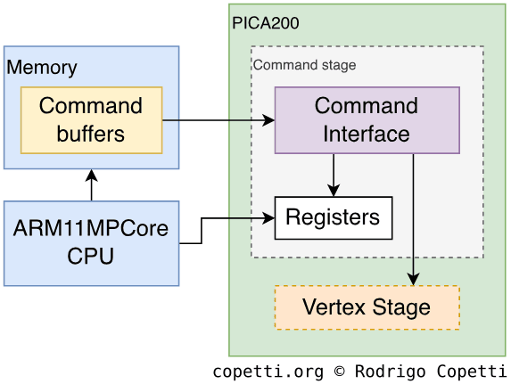
This is Nintendo’s first portable console to finally draw triangles in ‘the usual way’. That is, with the use of commands. But it’s not a surprising factor, as the PICA200 is expected to abide by the teachings of OpenGL ES.
In essence, the PICA200 draws polygons by reading a command buffer [31]. Furthermore, the vertex data can either be embedded within the command or stored in a separate buffer in VRAM, with the latter being the most efficient.
Vertex
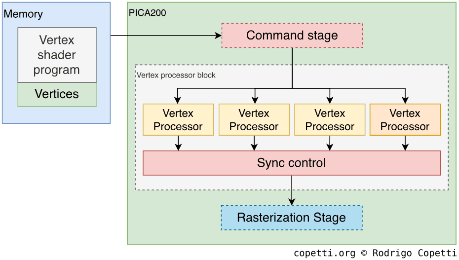
The PICA200 provides four Vertex Processors (VP) that operate in parallel. However, if the geometry shader (the next pipeline stage) is activated, only three processors can be utilised.
Each core computes 96-bit vectors made of four 24-bit floating-point values [32], but unlike the ARM11’s VFP, they don’t comply with IEEE-754 [33]. The vertex processors are programmed using assembly language specific to the PICA200 (reminiscent of the days of the Nvidia NV30) and are operated as follows [34]:
- Developers write the vertex shader using PICA200 assembly. For reference, the instruction set is very similar to Microsoft’s
vs_2_0[35]. - The shader is compiled using a proprietary assembler.
- The 3DS program must copy the compiled binary to memory (either FCRAM or VRAM).
- Then, the 3DS program issues a GPU command to load the binary and connect it with the program.
Once the vertex cores finish processing, they output the results to the Sync Control block, which acts as a vertex cache and buffer. It has a capacity of 384 Bytes, enabling it to hold up to 32 96-bit vectors. Finally, the next stage reads from this block.
Geometry
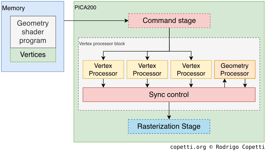
The geometry stage is a signature feature of 8th-generation consoles, allowing developers to spawn complex geometry out of simple vertex data.
In this case, the PICA200’s geometry stage is implemented by stealing one of the four Vertex Processors. Then, the ‘geometry’ vertex core is loaded with a different vertex shader. Finally, it receives the vertex data from the three other processors.
Examples of uses for the geometry shader include square or line generation (using point primitives), geometry subdivision, silhouette edge rendering; and random particle generation.
Rasteriser
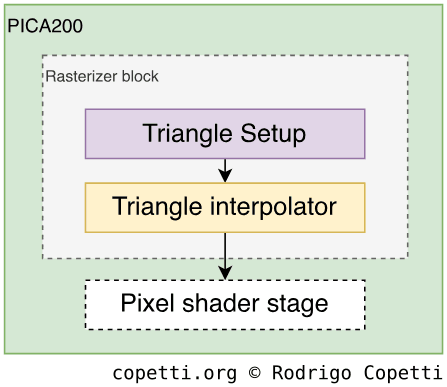
At this stage, all primitives are converted into pixels.
The rasterizer unit on the PICA200 is very simple, it just generates triangles out of primitives, then applies culling and clipping to remove unseen triangles (hidden behind others and/or outside the view area, respectively). This is all very similar to OpenGL ES’ modus operandi, albeit developers have to watch out for some coordinate systems that are inverted when working with the PICA200.
Fragment
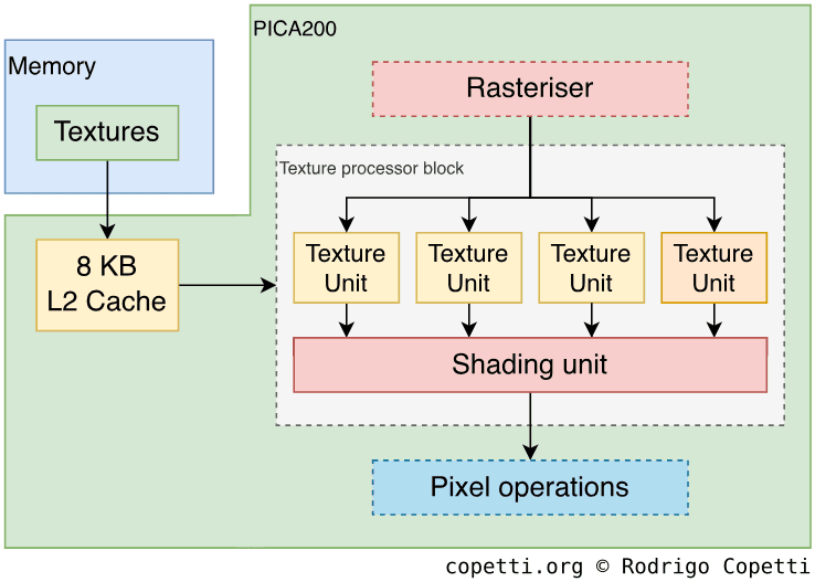
The fragment stage is made of two areas: the texture units, which can fetch textures in memory and process them. And the shading unit, which can perform extra operations on the texture data.
The PICA200 contains four texture units [36], each houses 256 Bytes of L1 cache and all of them share 8 KB of L2 cache. However, the units are not homogenous. Instead, the range of services varies between each unit [37]:
- Only three units can process 2D textures.
- Only one unit can perform shadow, cube and projective texture mapping.
- The last unit is more of a noise generator, meaning it only outputs random textures. It uses a combination of a random number generator and a colour lookup table. This is a slender yet efficient way of implementing procedure generation with textures, saving bandwidth along the way.
Afterwards, it’s the job of the shading unit to creatively fiddle with the textures coming in. However - and something unexpected considering we’re talking about an 8th-generation console - is that the PICA200’s unit is not programmable with pixel shaders [38]. Instead, we find six configurable colour combiners, each combiner receives three RGB or Alpha values and performs a logical operation on them. The result is passed to the next combiner and so forth. Each colour combiner can get its input from the previous combiner (except the first), a texture unit or a constant value.
All in all, a modern reflection of the Flipper era (while abiding by the OpenGL specification [39]), but don’t forget developers may also combine this with the aforementioned Maestro functions.
Post-processing
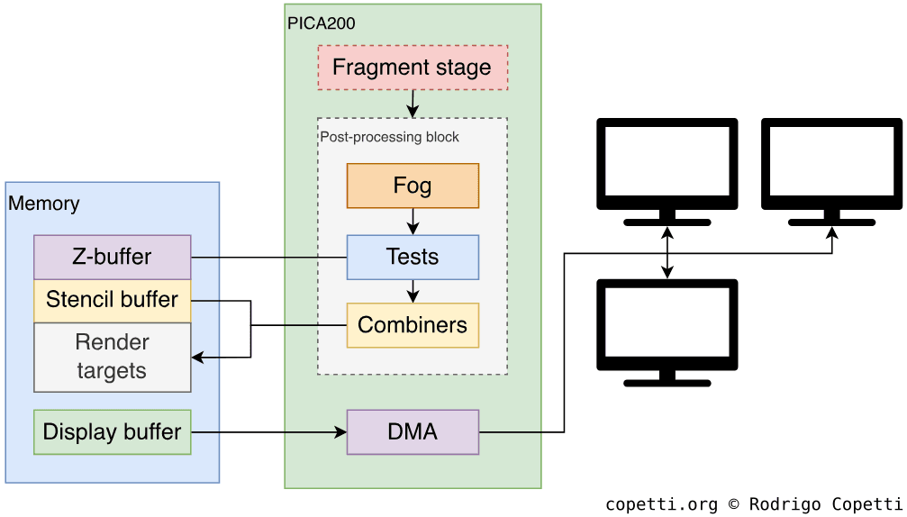
After the frame is processed and ready to be written into the framebuffer (or render targets), it goes through a sequence of final ‘corrections’. This is similar to the OpenGL ES 2.0’s pipeline.
That being said, the frame goes through alpha, stencil and depth testing. Afterwards, the result can be mixed with an existing frame (in the framebuffer) using the colour blender or logical operators (AND, XOR, etc.). Finally, the frame is written into the assigned buffer in memory either as a whole or through a stencil filter (for masking).
For additional smoothing of the edges, the PICA200 can render the framebuffer at twice the selected dimensions, and then average it with antialiasing 2x2. This is an old technique known as supersampling.
Once the framebuffer is ready to be displayed, it must be copied into another block in memory called LCD frame-buffer (whose format is better aligned to the scan-line procedure of the LCD screen) and then transferred to the LCD in the form of scan-lines.
Interactive comparison
Now that you’ve seen how the PICA200 draws its triangles on the screen, it’s time for some practical examples. Here I’ve gathered two Marios from Smash Bros games, the Wii and 3DS one. Notice how the perceived level of detail of the newer ‘angry Mario’ is very close to its home console equivalent.

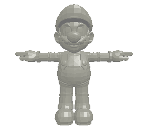
 Interactive model available in the modern edition
5,455 triangles.

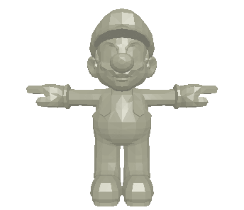
 Interactive model available in the modern edition
3,080 triangles.
It’s worth reminding again that, in practice, the PICA200 will be rendering three screens at the same time, something that the Wii’s GPU wasn’t subjected to.
Hidden additions
The ‘New’ 3DS variant also appears to bundle an uncommon DSP called MVD. It performs H.264 & MJPEG decompression and YUV-to-RGB colour conversion [40]. The CPU programs it by writing to its registers. In turn, the MVD houses a dedicated DMA unit to process the data in FCRAM independently.
Overall, there isn’t extensive documentation about this component and I can only presume it resides somewhere in the SoC. The Web Browser found on the New 3DS seems to be its only consumer (for accelerated video playback).
Nostalgic rendering
After all that’s been explained, there’s one question left unanswered: How does the PICA200 render Nintendo DS and Game Boy Advance games? You may remember that the DS and GBA’s GPU exhibit completely different modus operandi for rendering and broadcasting frames.
The explanation is that the DS and GBA PPUs are housed in the SoC and DSi/DS/GBA games will operate them as they originally did on previous consoles. The PPUs output (scanlines) is delivered to a block called LgyFB, which may optionally upscale the frame, and then forward it to the framebuffer, where the PICA200 will take care of displaying it. It’s the job of the ARM11 and its DMA to take care of all memory transfers during this process.
Naturally, this arrangement will add some delay (a.k.a. lag), albeit negligible to the user.
Audio
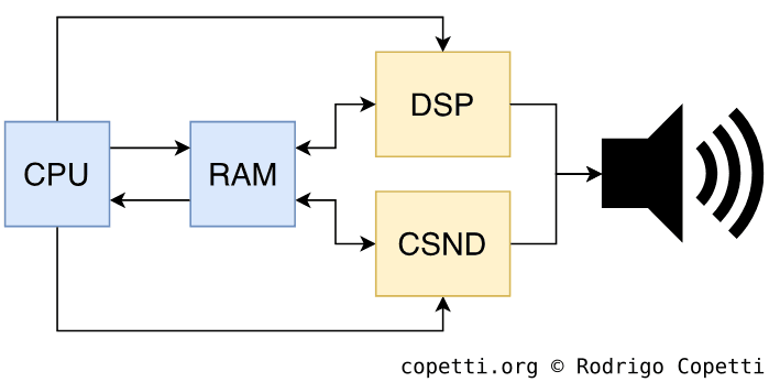
Overall, the SoC houses two audio blocks:
- A proprietary DSP exclusively programmed for sound operations. This is used by 3DS games.
- A variant of the Nintendo DS audio block named CSND. 3DS, DS and GBA games use it.
The 3DS-only hardware
You may know that this same DSP was previously bundled with the Nintendo DSi, but treated as an optional accelerator instead. With the 3DS, it’s become the designated audio processor, so it’s no longer a voluntary component.
The DSP is called CEVA TeakLite II [41] and operates at ~134 MHz [42]. It’s manufactured by ParthusCeva, a company that provides synthesisable cores for audio processing [43], and I guess ‘synthesisable’ was the keyword Nintendo was looking for when they partnered.
Moving on, the DSP outputs stereo samples (2 channels) of up to 32 kHz of sampling rate and 16-bit resolution.
Next to this component, we can find 512 KB of RAM that is used by the DSP as a working area. It’s double-buffered (256 KB per buffer), so both the CPU and DSP can read and write without interruption [44]. Apart from that, the DSP comes with a dedicated DMA that can transfer data in and out of those 512 KB.
Operation
For all intents and purposes, games treat this as an opaque DSP. Thus, only Nintendo knows how to program it.
3DS programs, as a consequence of being developed using the official SDK, bundle a DSP firmware (solely authored by Nintendo) which is then uploaded to the DSP chip at runtime [45]. Afterwards, programs rely on that firmware to execute audio-related routines. Furthermore, the audio services provided by the operating system further abstract the communication between the program and the DSP’s firmware [46].
In any case, while the DSP firmware may change over the years, some capabilities have remained the same. For instance, the DSP can mix ADPCM and PCM samples. with support of up to 24 channels [47]. There’s also functionality for filtering and sequencing, including the generation of PSG-like sounds.
Interestingly enough, the steps followed for hacking the 3DS (so it can execute homebrew application) optionally involve extracting the HOME Menu’s DSP firmware, so homebrew may use it to provide audio output [48].
The backwards-compatible block
At the other end of the spectrum, we find the CSND block. 3DS may use it as an extension of the DSP and DS/DSi/GBA games rely on it to replicate their hardware.
In terms of functionality, the CSND features 32 channels [49], which is twice the amount of the Nintendo DS counterpart.
Curiously enough, early homebrew defaulted to this block for providing sounds, while waiting for the DSP to be reverse-engineered.
Pipeline
Both DSP and CSND work independently and separately output their audio to the speaker.
As a curious note, the original Nintendo 3DS didn’t play well with the speaker’s capabilities, as Nintendo ended up providing troubleshooting guides for cases of buzzing noises and fluctuations with 3D slider [50], all caused by the design of the case.
I/O
This section tends to be very rich in technologies considering Nintendo’s consoles favour generous I/O before state-of-the-art CPUs and GPUs. Let’s see what the Nintendo 3DS offers.
External interfaces and peripherals
The Nintendo DS had tons of modules built-in and the Nintendo DSi added more on top of it (after removing the GBA Slot). Now we find ourselves with a new console combining interfaces from two decades (the 2000s and 2010s).

To be fair, we still don’t have a standard like USB, but that may be expendable considering the Nintendo 3DS bundles the following:
- A keypad composed of digital buttons, an analogue circle pad.
- 3D and volume sliders.
- A Wi-Fi switch.
- A resistive touch sensor on the bottom screen.
- A gyroscope measuring the console’s rotation changes.
- An accelerometer to measure the console’s motion.
- One front camera and two back cameras, the latter allowing to take stereoscopic pictures.
- An infrared transceiver, used to transfer data between external accessories.
- An SD card slot, serving as external storage.
- A standard 3.5 mm jack socket for headphones.
- A game card reader, where 3DS, DSi and DS retail games are read from.
The ‘New’ enhancements
If that wasn’t enough, the New 3DS came with more modules on top. This includes:
- Two extra digital buttons and an extra analogue circle pad (called ‘C-Stick’).
- An NFC Reader on the bottom screen.
- An infrared LED, reserved for head tracking.
- The SD slot is replaced with a microSD slot.
- The Wi-Fi switch has been removed, now it’s only controlled through software.
Now, to prevent leaving ‘old’ users behind, Nintendo provided external accessories to enhance the old models, although most of them relied on the single infrared transceiver to connect. Thus, only one accessory could be connected at the same time.
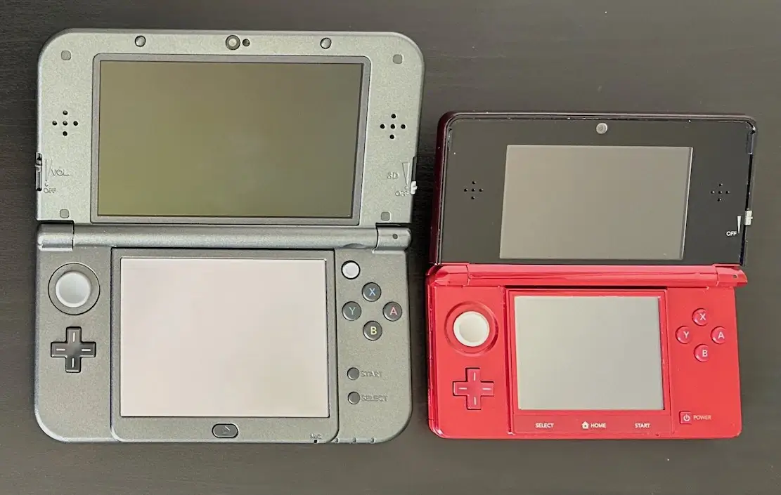
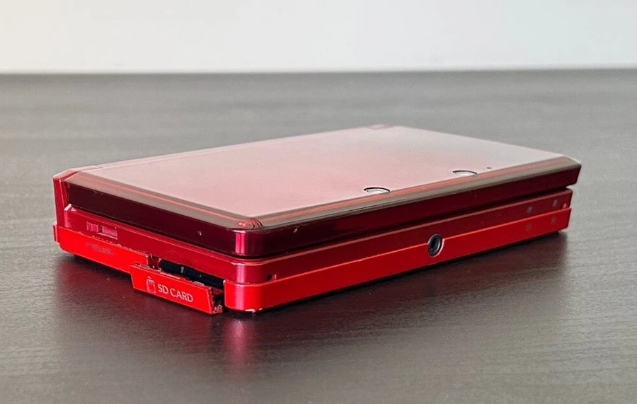
Not all the exclusive features of the New 3DS can be replicated, however. For instance, the New 3DS’ head tracking mechanism depends on the extra ARM11 core.
Internal interfaces
Now it’s time to check how are these interfaces - and others - internally wired up.
Firstly, a large subset is interconnected with the standard Serial Peripheral Interface (SPI) protocol. There are four SPI buses and all of them are accessed by the ARM9 (which I assume also includes the ARM7). The ARM11 only has access to most of them [51]. In any case, the SPI buses connect the following modules [52]:
- The flash memory found inside 3DS game cards, for storing save data.
- DS’ Power Management.
- Parts of the Wi-Fi chip.
- Touch screen.
- Sound.
- Microphone.
- Circle Pad.
Curiously enough, some peripherals are interfaced twice to replicate the old DS/DSi’s I/O layout and also provide extended capabilities for 3DS software.
Secondly, there’s a Human-interface device (HID) module connected to both ARM11 and ARM9 data buses. This is how the digital keypad is accessed. The data is read through a 16-bit register.
Moving on, we got an I²C block which uses a more sophisticated serial protocol. This is connected to the following [53]:
- Front camera, also works in DSi mode.
- Two back cameras, the right camera is accessible in DSi mode as well.
- Infrared transceiver.
- The NFC interface, in the case of the New 3DS.
- The ‘QTM’ module, used for head-tracking (New 3DS only).
- Gyroscope.
- MCU chip, a separate controller that interfaces more components (explained in the next section).
Finally, there are various registers interfacing FIFO blocks which, in turn, connect to two relatively high-speed (16 MB/s) peripherals [54]:
- Internal eMMC memory.
- SD card slot.
The supplemental computer
As confusing as it may sound, there’s more hardware left to discuss. The rest is handled by a middle-man chip called Auxiliary Microcontroller (MCU) [55]. This is just a microcontroller designed by NEC and manufactured by Renesas. Particularly, the model 78K0R, which bundles a proprietary (yet low-power and relatively modern) processor and a ROM [56]. The 78K0R stores a firmware handled by the console’s operating system, both ARM9 and ARM11 can interact with it but so do other peripherals.
The MCU chip exclusively controls the following [57] [58]:
- Accelerometer.
- LCD screens.
- LED indicators.
- Power Management.
- Battery fuel gauge and rejection (whether to enable the charging circuitry or not).
- Wi-Fi’s EEPROM.
- Real-Time Clock (RTC).
- 3D slider and Wi-Fi switch, the latter is only found on old 3DS models.
- HOME and power buttons.
A subset of this group is already accessible by the main CPUs. This is because the MCU also perform monitoring tasks, thereby saving resources from the ARM11 or ARM9.
Ready for trends
With such a heavy list of I/O hardware, you can now see how Nintendo tried to compete against the smartphone market. This led to interesting services deployed throughout the console’s lifecycle:
- A QR Reader bundled with the camera app.
- AR Games: Nintendo shipped ‘AR Cards’ that could be scanned with the 3DS camera using an app called ‘AR Games’. This would make static Nintendo characters pop up in your room, like any traditional augmented-reality-based application.
- Face Raiders: Another camera-based app, but in this case, takes a photo of the player to compose the game’s characters. The player must then use the gyroscope and microphone to battle his/her evil clones.
- Amiibos: Uses the NFC reader to scan figurines and unlock game bonuses, the same service was also implemented in the Wii U.
- SpotPass: The continuation of WiiConnect24, now automatically connects to unsecured Wi-Fi access points.
- StreetPass: Automatically exchanges data between nearby 3DS systems. Nintendo marketed it as a way of connecting random 3DS players on the street.
- Play Coins: Unlocks game content by doing some exercise (walking).
Operating System
Having a large number of CPUs eventually impacts the overall complexity of the operating system. Not only that, but this console also stores more than one OS. This originates as a mechanism for providing large services (i.e. DSi/DS/GBA backwards compatible, rescue mode, etc.).
So, to avoid making this section any more confusing, let’s go by steps.
Architecture
The Nintendo 3DS, as a whole, comes with four firmware [59]:
- NATIVE_FIRM: Operates the console in ‘native’ mode (with the functionality exclusive to the Nintendo 3DS). Here, the ARM11 executes the main program.
- Curiously enough, there are two instances of NATIVE_FIRM installed (named FIRM0 and FIRM1, respectively) in case the first one gets corrupted, for some reason.
- This firmware is often referred to as ‘Horizon’ as well.
- TWL_FIRM: It commands the Nintendo 3DS to behave like a Nintendo DSi. It does come at the expense of disabling all the exclusive features, but considering how the CPU, GPU, sound and I/O are intertwined; TWL_FIRM is truly a work of art. Consequently, the ARM9 and ARM7 are placed in the foreground (they execute the main program) [60].
- The name ‘TWL’ comes from the codename of the Nintendo DSi.
- AGB_FIRM: Similar to TWL_FIRM, the 3DS now becomes a Game Boy Advance. Here, the ARM7 executes the main program.
- SAFE_FIRM: Used solely for maintenance-related tasks, such as system updates. This firmware is basically an early revision of NATIVE_FIRM (doesn’t go beyond version
3.0on the old 3DS and version8.1on the New 3DS [61]).
All of these firmware come with separate binaries for the ARM11, ARM9 and ARM7 CPUs. The only exception is that the ARM7 won’t be active under NATIVE_FIRM and SAFE_FIRM.
Generally speaking, the Nintendo 3DS will first launch a Boot ROM and then bootstrap NATIVE_FIRM. Afterwards, the running operating system may choose to reboot to another firmware based on the user’s actions (i.e. load a Nintendo DS game or run the firmware update assistant).
Let’s take a look now at how each CPU behaves in NATIVE_FIRM mode.
The security processor
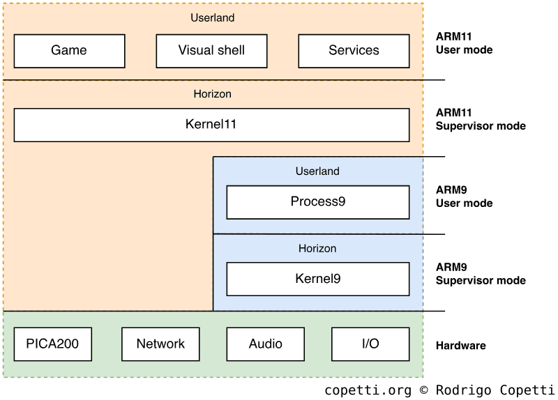
Once NATIVE_FIRM is bootstrapped, the ARM9 runs its own operating system made of a kernel called Kernel9 and a single program called Process9 [62].
Kernel9’s design follows the microkernel model, meaning it only provides essential abstraction with the hardware, including:
- Memory management.
- Process scheduling.
- Inter-Process Communication.
On the other side, Process9 is a userland application that implements these services:
- Communication with the ARM11, called ‘PXI’.
- Cryptography-related functions. This involves AES, RSA, SHA and ECDSA.
- I/O management.
- File System.
- Title (3DS software) verification and installation.
Both Kernel and Process9 reside on an ARM9-only block of 1 MB of SRAM (1.5 MB in the case of the New 3DS).
In terms of security, there’s no privilege distinction between Kernel9 and Process9, since the latter has unconditional access to a system call that runs arbitrary code in kernel mode.
In summary, combined with the exclusive I/O hardwired into the ARM9, this CPU has the role of a security processor, much like what the Wii and Wii U’s ARM9 also did, and unlike the co-processor architecture of the Nintendo DS, where its second processor just offloaded I/O and audio tasks.
The user processor
Likewise, the ARM11 runs a kernel of similar architecture to the ARM9 one (now called Kernel11). The big difference is that the ARM11 will be running multiple userland processes, and in doing so they provide services like:
- Communication with the ARM9, called ‘PXI’.
- Multi-core processing.
- Networking, HTTP and SSL.
- Connection with Nintendo online infrastructure.
- The graphical shell (called ‘HOME Menu’).
- The ability to launch applications.
- A layer of abstraction for apps called Services, which games must call to access hardware resources. Some components like the GPU are interfaced by a very thin API, nonetheless.
- Furthermore, services are implemented in a layered manner. Games only access a subset of these, and the latter in turn invokes greater privileged and specialised services.
The ARM11’s kernel resides on a dedicated block 512 KB of SRAM [63], also called ‘AXI Work RAM’ or ‘AXI WRAM’, because it’s connected to the ARM11 using the AXI protocol.
Imposed behaviour
Now for the bitter news, NATIVE_FIRM also enforces unusual restrictions on user programs.
To start with, the ARM11’s scheduler is hard-coded with specific behaviour for each core (as opposed to treating every core as general-purpose units):
- The first core, called appcore, is for the game to use. Yet, its thread scheduling policy is FIFO, meaning that the game can deadlock itself if multi-threading is improperly used [64].
- The second core, called syscore, gets assigned system-related tasks.
Conversely, syscore can lend 30% of its execution time to user applications, which may be helpful to offload some operations, although not every routine may work under syscore (especially time-sensitive ones) [65].
The curtailment is further extended with the New 3DS, whose ARM11 MPCore now comes with four cores, namely:
- The fourth MP11 core is solely used for face-tracking. Instead of adding circuitry, Nintendo engineers implemented face-tracking through pure software. Thus, it reserves one MP11 for this. I’m guessing this was a cost-effective solution for Nintendo.
- The third MP11 core is predominantly idle [66]. This is because, by default, the scheduler is not programmed to dispatch threads there. Game meta-data does include a flag that enables thread scheduling on the third core, albeit its adoption has only been confirmed in Xenoblade Chronicles 3D [67] (a game exclusive for the New 3DS, incidentally), so far. It’s possible that, at one point, Nintendo considered a more seamless approach, but ultimately found it unfeasible due to battery consumption concerns, and perhaps compatibility issues with games optimised for either setup.
- Considering the New Nintendo 2DS XL is a ‘New’-type variant without the stereoscopic screen, this means that, for the most part, half of its quad-core CPU is wasted!
- CDMA, the ‘New’ DMA unit, is only accessible during the console’s boot [68]. After the boot process finishes, CDMA is never used again.
Moving on, in terms of usable RAM for games, we know that the Nintendo 3DS and New Nintendo 3DS come with 128 MB and 256 MB of FCRAM, respectively. What you need to know now is that the available RAM for apps is only 64 MB and 124 MB [69], respectively. This means that the OS consumes ~50% of the console’s main memory, not a particularly pleasant quality! To alleviate this, games also have the option to set a flag in their metadata (called APPMEMTYPE) to claim more FCRAM from the system, up to 96 MB and 176 MB, respectively. Behind the scenes, that flag instructs the system to reboot the console and boot the game without launching the HOME Menu beforehand, saving memory along the way.
All things considered, you can now sense how not all extra hardware in the New 3DS will automatically imply faster software. It’s a shame, and it gives me the feeling that the New 3DS was a rushed product, from the software perspective. But to be fair, Nintendo never planned the ‘New’ 3DS to be a full successor of the original 3DS. The ‘New’ brand was a clear move to refresh the 3DS line, considering the sales number wasn’t satisfying, to say the least.
Storage Medium
Now that we know how the operating system is designed, let’s look at where and how data is stored in this console.
Boot ROMs
Following its long ancestor, the Game Boy, the SoC stores a series of unencrypted ROMs containing the programs used for booting up NATIVE_FIRM [70]. These bootstrappers are called Boot9 and Boot11; and are executed by the ARM9 and ARM11, respectively. Likewise, they are physically and virtually kept hidden for security reasons. To give you an example, Boot9 stores AES decryption keys, which are not something to carelessly leave anywhere.
Interestingly enough, Boot9’s code has revealed that it’s more capable than just bootstrapping NATIVE_FIRM from eMMC NAND. However, due to certain routines having hardcoded directories and security layers added on top, the only firmware the Boot ROMs can ultimately load is NATIVE_FIRM from eMMC NAND.
Moreover, while multiple components have changed with the arrival of the New 3DS, the BootROMs have not changed a bit [71].
OTP memory
To further increase the level of security, the console stores a series of console-unique information in One-Time-Programmable (OTP) memory [72]. Similarly to the Wii and Wii U, this information also includes encryption keys.
OTP is written once during manufacturing, so the keys differ between each console. Hence, one hacked console won’t necessarily be able to compromise the rest. This is a significant milestone for a portable console, considering a certain previous implementation included global keys.
eMMC NAND
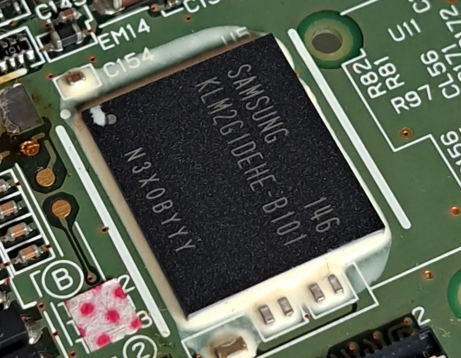
Next to the big SoC, there’s an eMMC NAND Flash chip. However, its size is slightly different depending on the manufacturer [73]. For instance, Toshiba supplied 943 MB and 1,888 MB chips, while Samsung provided ones with 954 MB and 1,240 MB.
To tackle this disparity, Nintendo defined the 3DS partition table using a common size: 943 MB for Old 3DS (Toshiba-size) and 1,240 MB (Samsung-size) for New 3DS. So, if your console came with a larger eMMC chip, the extra space is unfortunately left unemployed.
In any case, the console relies on eMMC for storing its system data, including the multiple firmware, and user data (saves and configs within 3DS and DSi mode).
SD/microSD
Once an optional (and sometimes, symbolic) medium, SD cards now enjoy similar responsibilities to internal storage, as the 3DS is dependent on it to download software from the eShop and store user data (game saves, camera pictures and microphone recordings) [74].
Software and user data stored here are protected with AES-128-CTR encryption.
Boot process
Now that we know how the operating system is structured and where data is stored, let’s see how the Nintendo 3DS goes from a glossy powered-off brick to becoming an operating console offering multiple services.
Multi-core chaos
Considering the 3DS must be able to manage four processors (2-core ARM11 + ARM9 + ARM7) in its SoC - or six, if you look at the New 3DS - one can only wonder how these ‘central’ processors suddenly become exceptionally coordinated during the console’s startup. Well, it’s all about implementing a master-slave hierarchy.
With the ARM9 and ARM7, there’s not a lot of room for doubt, both can be powered on separately and load different binaries. So the challenge is mainly focused on disseminating the homogenous multi-core ARM11.
In the ARM11 MPCore cluster, all cores start execution at vector 0x00000000 [75]. However, CP15 (the System Control co-processor) provides a register called CPU ID which, among other things, serves to identify the core currently executing instructions. Thus, programmers can query this register to decide whether the current CPU core should give orders (master) or wait for commands (slave). ARM later improved this technique by supplying a dedicated register called mpidr, found in ARMv7 CPUs.
Thanks to this, Nintendo engineers were able to identify any CPU core within the 3DS cluster and implement a bootloader where all cores become coordinated, and then carry out the necessary functions to bring the console to life.
Boot procedure
Time to dive into the boot process. As with any other console of its generation, security is of great importance, which will have an impact on the boot stage. To avoid making this section too dense, I’ve simplified the stages where the security system is set up, but you’ll find more information in the ‘Anti-piracy’ section.
Having said that, once the console is powered on, the following sequence of events takes place [76] [77]:
- The ARM9 and ARM11 power up.
- The ARM9’s reset vector is at address
0xFFFF0000, which points to Boot9 [78]. The ARM11 is induced in an infinite reset until its reset pin is lifted. - Boot9 clears ARM11’s reset pin and then initialises the ARM9’s MPU.
The ARM11 MPCore will now start execution of Boot11 in parallel:
- ARM11’s reset vector is at address
0x00000000[79], which happens to be in the same place as Boot11. - Boot11 will branch depending on which core it is being executed on. If it’s greater than core 2, it hangs indefinitely.
- Wait until ARM9 is finished bootstrapping a firmware.
Meanwhile, the ARM9 will be busy continuing with Boot9 execution:
- The AES and RSA public keys are exported to the AES and RSA engines (these will be explained in the ‘Anti-piracy’ section).
- Boot9 will try to boot from NAND.
- In NAND, there’s a partition at location
0x0called ‘NCSD header’, this states that there are eight partitions, each with a firmware to boot from. - For each firmware partition listed, Boot9 will fetch its header, validate the SHA-256 hash and RSA-2048 signature (using a set of keys previously loaded from BootROM) and repeat this process until one validation succeeds. Then, it will boot from there.
- In NAND, there’s a partition at location
- If all validations in NAND fail, Boot9 will try to boot from a Flash memory in the Wi-Fi module. If that also fails, the console will display an error screen.
- The first partition validated happens to contain NATIVE_FIRM. Boot9 will proceed to copy the firmware to different memory areas based on the header’s parameters.
- Disable half of Boot9 and Boot11. In doing so, FCRAM will be accessible.
- Redirect ARM9 and ARM11’s execution to the firmware’s entry points.
Now that NATIVE_FIRM is bootstrapped:
- The ARM9 will:
- Load Kernel9.
- Kernel9 hides OTP memory and loads Process9.
- The ARM9 CPU is now up and running Process9.
- Whilst the ARM11 does the following:
- Load Kernel11.
- In the case of the New 3DS, Kernel11 will write to a new register called
CFG11_BOOTROM_OVERLAY_CNTto overlay Boot11 code [80]. This will allow to redirect execution of the new ARM11 cores (core 3 and core 4) away from Boot11 to arbitrary functions in Kernel11, thereby taking control of them. - Kernel11 will start various system processes, including PM (Process Manager).
- PM will start the ‘NS’ (Nintendo User Interface Shell) system module.
- NS will either launch a game or the HOME Menu application.
- The user is now in control.
Alternative boot processes
All of the previous explanations have been focused on booting up NATIVE_FIRM, which results in the traditional native 3DS mode. For other firmware such as TWL_FIRM, AGB_FIRM and SAFE_FIRM, it’s a bit more complicated. Turns out the previous boot process is still needed because only NATIVE_FIRM can be booted from a power cycle. But once this is running, it can bootstrap any of those firmware, and each will program the ARM9 differently. In either case, the security set-up during Boot9 will still be enforced.
TWL_FIRM and AGB_FIRM, in particular, operate a special set of registers that mould the 3DS hardware and memory layout in accordance with what DS, DSi or GBA games expect to find. FCRAM can still be accessed, allowing to boot a game ROM from those places as well (apart from the NTR card reader). However, FCRAM will be reconfigured to follow the DS and GBA bus specification (16-bit wide, instead of 32-bit).
A big difference about the backwards compatible firmware is that, at last, the ARM7 will be active (as Nintendo DSi/DS and GBA software require it).
To exit either mode, non-NATIVE firmware contain a routine that reboots the system and consequently returns it to NATIVE_FIRM. Thus, 3DS mode.
Interactive shell
The 7th generation of console interfaces has landed on the Nintendo 3DS. A clear indication is that users don’t need a retail game to make the most out of their console, just navigate through the shell and you’ll find numerous apps and services bundled. This includes the special offering of this console (3D camera, stereoscopic view and augmented reality). The pressure to compete against smartphones couldn’t be clearer.
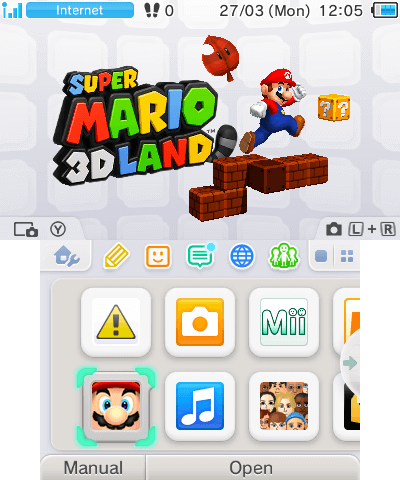
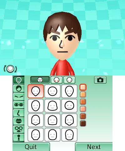
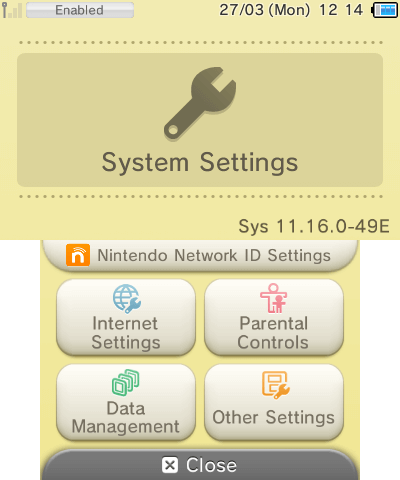
In terms of user interface design, I’m inclined to say there are many patterns borrowed from the Wii System Menu, yet ported to a dual-screen portable system. The HOME Menu (name of the interactive shell) uses a 1-page navigation system where every installed application is shown on a scrollable grid. Except for a few shortcuts here and there, every service is an application to be launched.
Now, being a Nintendo product, you can expect a special focus on creativity and attention to detail. Families are the target audience, nevertheless, adults are the ones paying, and Nintendo knows that.
Maintaining consistency
The NS module is not only responsible for launching the interactive shell, it also offers 3DS software with the ability to invoke routines to handle certain interactions. One example is the ‘Back to HOME Menu’ overlay, which must be shown whenever the user presses the ‘HOME’ button.
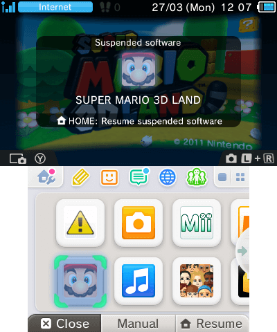
Furthermore, 3DS software may also invoke ‘mini applications’ for attending other events (i.e. show the virtual keyboard), these are known as Applets [81].
Both sets are a crucial dependency for all applications, as they are responsible for properly reacting to external events consistently. Interestingly enough, since Applets and NS routines are not part of the game itself, in the case of New 3DS systems, even if a game is running in compatibility mode (that is, with all the ‘New’ hardware disabled), they will still be executed using the full extent of hardware, giving a small performance boost to unoptimised 3DS games.
The legacy shell
Whilst the special firmware includes the old BIOS routines DS/GBA games will expect, there’s no DS or DSi shell in sight.
The old Wi-Fi setup screens (invoked by DSi and DS games) are the only exceptions. Interestingly enough, while the original DS Wi-Fi settings are useless (as they can only connect to WEP-protected access points), the DSi counterpart (accessed from DSi and ‘DSi enhanced’ DS games) can alter the 3DS’ Wi-Fi settings. Yet, these games bundle an old Wi-Fi driver that only worked with the real DSi (the 3DS contains an Atheros AR6014 while the DSi came with an Atheros AR6002 or AR6013). So, to tackle this, both Wi-Fi settings are automatically synced when the firmware boots up [82].
Updatability
Well, of course, an updatable system is pretty much a requirement, not only for providing new functionality but also from a security perspective.
You can update the system software either online or through a game cartridge. Confusingly enough, both contain different update packages. Game cartridges only bundle system updates without the updated user apps, whereas network updates include everything [83]. Consequently, version names encode a mix of the two, in case the user used both channels.
To install updates, the NS service reboots into SAFE_FIRM, where the System Updater takes care of this process [84].
Games
It’s time to check how game development and distribution were carried out. Additionally, we’ll see some exclusive services Nintendo prepared for this console.
Development ecosystem
Before the Nintendo 3DS arrived, developing for embedded system involved monumental efforts and high levels of patience. Compared to desktop applications, the tooling wasn’t standardised and sometimes it didn’t converge well with each other (ActiveSync is the clearest example I remember). The range of documentation didn’t usually go beyond what the manufacturer provided, the same applied for technical support.
Entering the 2010s decade, and coinciding with the influx of an ARM-based smartphone industry and more efficient compilers, development for those platforms was no longer a complicated endeavour. Consequently, game studios developing for the Nintendo 3DS were able to enjoy this evolution. Now, Nintendo was not providing a standard toolchain yet, but they were on the right track (finally reached with the Nintendo Switch).
Curiously enough (and this is an interesting contrast), back in 2011, Apple offered Clang/LLVM 1.3 and OpenGL ES 3.0 for developing iOS apps, this was considered state-of-the-art for mobile projects. Well, you’ll see throughout this section that this wasn’t the case for Nintendo. Yet, at present, if you grab an old iPhone 4s and try to install any app on the App Store (its only official medium), it will tell you your system is too old. Whereas you can still play any retail game on your 3DS. Food for thought.
Hardware Kits
Nintendo partnered with two suppliers to produce development kits [85]. The first supplier was the well-known Intelligent Systems and the other was Kyoto MicroComputers.
Among the many options, studios could rent a general-purpose ‘CTR-BOX’. This is a metallic box housing the 3DS hardware, and connected to it is a ‘dummy’ 3DS case that serves as a controller and display. With it, developers could deploy, test and debug their code.
For more single-purpose tools, studios could get official flashcards to distribute game prototypes to external testers. These flashcards still only run on non-retail equipment, though this included cheaper options (with reduced functionality) than the fully-fledged CTR-BOX.
With the arrival of the New 3DS, IS and Partner offered the ‘SNAKE’ kits with updated hardware.
Software Kits
As always, licensed studios would also get an SDK package from Nintendo which included [86]:
- A variant of
armcc(ARM’s C and C++ compiler) modelled for the Nintendo 3DS and the ARM11 MPCore.- This will just produce code for the ARM11 MPCore. Both ARM9 and ARM7 are out of the equation, as 3DS games only run within the ARM11 cluster.
- Debuggers made for IS and Partner’s development kits.
- APIs to communicate with the hardware and operating system’s services.
- Four graphics libraries:
- GL: a simpler but slower OpenGL ES API.
- GD: a faster alternative to GL that generates PICA200 commands.
- GR: the closest-to-metal PICA200 command API, albeit with the steepest learning curve.
- GX: the general-purpose library used for PICA200 management.
- A 3DS app packager, so an executable can be created.
- Further libraries to ease common development tasks, such as implementing network protocols, online gaming and audio/video decoding and processing.
- A plugin for Visual Studio 2010, so it can be adopted as the main IDE.
- Assistant tools for the PICA200.
- Profilers, for measuring and optimising performance.
If that wasn’t enough, developers also had access to NintendoWare to download code samples, libraries and further tools designed for Nintendo 3DS development. Furthermore, with the arrival of the New 3DS, game engines like Unity lent their support to this (once ignored) platform [87].
Medium
The Nintendo 3DS can run software from three different media.
Gamecards
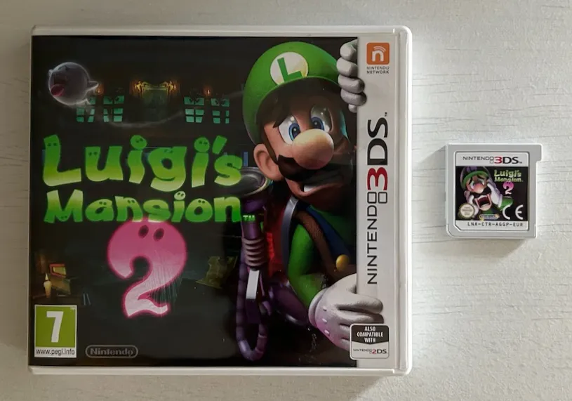
This is the distribution channel for retail software. Internally called ‘CTR cards’, they’re just another proprietary card/cartridge designed by Nintendo. To be fair, they’re not very different from NTR Cards (used by the Nintendo DS), aside from a cosmetic notch at the top right. Inside them, there is read-only and/or writable storage.
The variants of CTR cards range drastically. Their PCB can bundle a ROM chip ranging from 128 MB to 4 GB in size, while also including some ‘backup memory’ to store saves, this can be either 128 KB or 512 KB. In other variants, the whole CTR storage is instead filled with Flash (up to 2 GB), and it’s partitioned to store both the game and saves in the same physical chip.
Moreover, since games will be bundling the official SDK as well, the usable capacity of ROM/RAM allowed to the game depends on the revision of the SDK linked to.
Internally, the ROM chip is connected to an 8-bit data bus [88], while the backup memory relies on a serial bus. Both are connected to a 16.6 MHz clock. When the card is inserted into the console, the 3DS first queries it using NTR (Nintendo DS) commands [89], and then switches to ‘CTR mode’ once it detects it’s a 3DS card.
eShop/SD Card
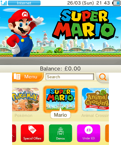
Expandable storage, an icon of the 8th generation of consoles. The Nintendo 3DS now enjoys installing and launching software from the SD (or microSD) card; and with it, retail cards are no longer the only medium for games. In fact, SD storage is the result of an emerging distribution channel: The Nintendo online store, bundled into every Nintendo 3DS.
Thanks to the eShop, there were new distribution techniques: users could pre-order games and DLCs before the shipping date [90]. These would get downloaded ahead of time, but can only be played once the release date arrived.
When it comes to storing the respective saves, Nintendo allows its downloaded software to request up to 1 MB of SD card storage. However, this rule is waived if the retail counterpart already requires more space, in which case the system will allocate as much ‘backup memory’ as the respective CTR card already provides.
Local wireless
Download Play, a debuting feature of the Nintendo DS that enabled players to transfer small games between their consoles, has been pushed into the Nintendo 3DS. It now comes with a revamped protocol that relies on a thick security layer, in line with the rest of the software executed in the new console.
I’d say the big difference now is that transferred games (or ‘demos’, for it’s worth), are now installed into NAND (as any other installable package) [91]. There’s only one slot reserved for them, so the installed program is replaced whenever a new game is transferred in.
Virtual console(s)
If, after all explained, users still got bored, Nintendo prepared another offering for them: Virtual Console.
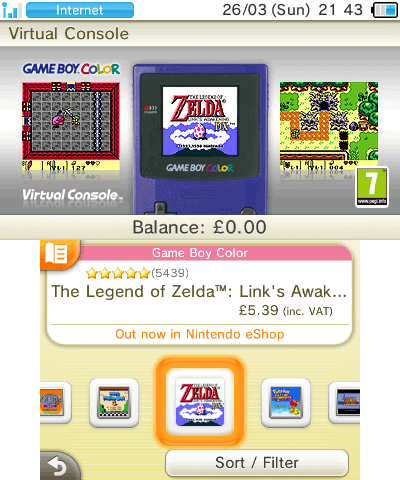
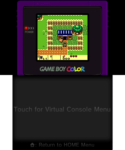
Once again, thanks to the bundled eShop app, Nintendo also expanded its 3DS-only catalogue by incorporating games originally published for the following consoles:
- Nintendo DSi (DSiWare only).
- NES/Famicom.
- Sega Game Gear.
- Game Boy.
- Game Boy Color.
Virtual Console games behave as any other application installed into the console. Except for DSiWare software, the application package includes a ROM and emulator. The latter implements interesting capabilities, such as Download Play (for some games) and save states.
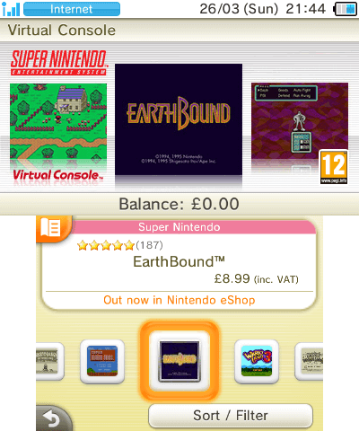
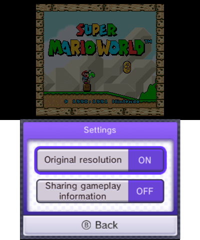
Once again, things were different for New 3DS users, as they could also access the Super Nintendo catalogue. This particularly strikes me as odd, as I remember a time when (homebrew) SNES emulators were developed for the original Nintendo DS (with its mere ARM9-ARM7 and a couple of megs of RAM).
Extra backwards compatibility
Now, here’s another peculiarity of Virtual console games: this console can also play Game Boy Advance games, officially. Yet, they’re not available for everyone. Only those who purchased a Nintendo 3DS before August 2011 (right before the console received an $80 price cut), became members of the ‘Ambassador Program’ [92]. One of the perks included access to a selection of GBA games which, for one reason or another, were kept exclusive until date.
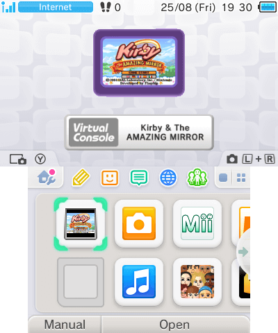
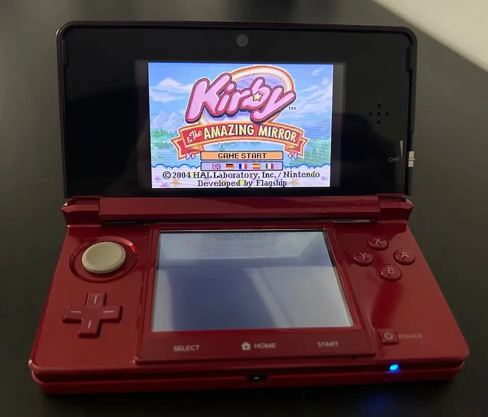
Even more puzzling, GBA titles don’t run on the ARM11 using an emulator (albeit there’s one installed, but never been used!). Instead, they kickstart the third firmware, AGB_FIRM, to run natively on top of the ARM7. In the end, these exclusive GBA games remained the only use for AGB_FIRM, as if Nintendo planned for something bigger in the future, but never materialised. This is another example of how the Nintendo 3DS possessed more hardware than the software ever took advantage of.
If you’re curious, GBA titles make use of the bundled ARM7 core instead. Thus, they don’t allow for the extra features that emulators (running on ARM11 cores) provide. Although, this happens at the exchange of running at full speed and precision. Be as it may, since the 3DS doesn’t contain a GBA cartridge slot, the GBA game is instead copied into FCRAM before the system reboots into AGB_FIRM, and then lets the ARM7 take control (while the ARM11 and ARM9 provide basic support tasks) [93].
With all these capabilities, and on top of being a portable console, one can’t help but wonder why Nintendo didn’t distribute GBA and Nintendo DS/DSi games on the eShop as well. Most probably a marketing and licensing issue, I sense.
Game updates
Another requirement of the 8th generation of consoles, games can now receive patches after the shipping date. That’s right, no more need to quality control the game before selling it!
Leaving irony aside, game updates are distributed through the eShop as well [94], which applies to all types of games (except Download Play). All updates are downloaded onto the SD card and eShop games get their updates applied altogether (along with the game itself).
Network service
Out with the old (Nintendo Wi-Fi Connection), in with the new (Nintendo Network)! The same service offered with the Wii U is also implemented on the Nintendo 3DS, and they’re admirably unified, so I recommend checking the Wii U article where it’s been explained in detail.
Anti-Piracy and Homebrew
The history of hacking this console is a long and interesting sequence of events. At first, interests focused on cracking game card readers (in an attempt to replicate the success of the Nintendo DS) and then shifted towards more sophisticated approaches, only involving the operating system.
Main targets
First things first, let’s start by describing the two main targets of this system:
- The Game/CTR card reader: This is where physical games are loaded. Historically, the Nintendo DS implemented a weak security mechanism that was eventually cracked and subsequently led to an influx of Flashcards.
- The Operating System: This area is responsible for verifying the authenticity and integrity of every single program before execution (aside from the Boot ROM). Disabling said mechanisms would grant the execution of Homebrew (unauthorised applications) without any restrictions, in theory.
They may look like two independent fronts (similar to the Xbox 360 and Wii U), but in the case of this console, both are intertwined. You’ll see it in a bit.
The card reader front
The card reader is the interface between the CPUs and the Gamecards’ memory chip. Its only job is to simplify the communication with the use of commands.
Inside the ROM/Flash of CTR Carts, the system will find a block of data in a secured format called NCSD, this will be handled by the operating system, who will be in charge of authenticating, validating and decrypting it.
In conclusion, it seems the OS is solely responsible for the communication with the card reader, so let’s move on to the next front.
The Operating System front
Before we continue, if you’re not familiar with symmetric and asymmetric encryption systems, I recommend reading previous articles of this series. They will also explain why systems like this rely so much on asymmetric encryption systems (such as RSA and ECDSA).
Dedicated hardware
You’d be right if you suspected that the ARM11 lacks the powerhouse to protect the whole system. Nintendo knew that too, so they took extra care and bundled extra components to compensate:
- The ARM11 cores implement the XN flag and the ARM9 bundles a Memory Protection Unit (MPU), meaning the CPUs won’t execute code from any location in memory just because the current program tells it to.
- As said before, the ARM9 acts as a dedicated processor to handle all security-related tasks while the ARM11 MPCore executes the game. Additionally, the ARM9 is exclusively wired to a few hidden cryptographic accelerators:
- An AES engine that performs AES-128 encryption/decryption without consuming (and exposing) CPU resources. This was inherited from the Nintendo DSi, but can now store up to 64 keys and can operate in numerous block cipher modes, including CTR, CCM, CBC and ECB [95]. Each key slot also features its own key-scrambler, meaning that two arbitrary keys can be used to generate the final AES key. Moreover, the key-scrambler won’t allow anyone to read the generated key, only to treat it as a blackbox to encrypt/decrypt data.
- An RSA engine. By contrast, this performs RSA encryption/decryption using a given RSA public key. This time, it only contains four key slots and there’s no key-scrambler [96]. However, it’s still a write-only space, meaning no one will be able to read the keys stored there. You’ll soon see that this system is filled with RSA-2048 and RSA-4096 signatures, which explains why this component is as crucial as the AES engine.
- A Pseudo Random Number Generator (PRNG): These are registers that return a different value every time they’re read from.
- OTP (one-time programmable) memory that stores console-unique keys, information about the console and CTCert (an ECDSA private key to authenticate with Nintendo’s servers). To complicate things further, these keys will be encrypted with an AES-CBC key found in Boot9. Finally, this region includes a flag to disable its access once it’s not needed anymore.
- Last but not least, the eMMC memory contains a register called CID (Card Identification) and stores unique information about the eMMC’s manufacturing, which will be fed to the AES’ key-scrambler for further obfuscation.
To top it off, everything is sealed in an SoC, including the two boot ROMs (Boot9 and Boot11). These are unencrypted, but since they’re inaccessible, they don’t represent a concern.
Chain of trust
This should come as no surprise considering we’ve already introduced RSA, AES and the boot ROM as part of the security system. To give you an overview of the Nintendo 3DS’ change of trust:
- ARM9’s boot ROM (Boot9) bundles the public key for decrypting and validating the contents of the NAND. The AES engine will be initialised with the keys stored in Boot9. With this, the contents of OTP memory will be accessed.
- The contents of eMMC are decrypted using Boot9’s AES keys combined with the eMMC CID.
- NAND and CTR cards are formatted using the NCSD format [97]. NCSD stores a header and a collection of up to eight partitions. The NCSD header contains a signature using RSA-2048 and SHA-256, which is quite strong. To decrypt this signature, the system finds its public RSA key in the boot ROM or ITCM memory (the latter was previously decrypted and copied from OTP). The choice depends on where the NCSD block came from (NAND or CTR card).
- Once the NCSD block is validated, the system accesses each partition. These are structured using the NCCH (Nintendo Content Container Header) format. Independently whether the data was pulled from NAND, the CTR card or the SD card, the NCCH block also contains an RSA-2048 + SHA-256 signature [98], and its payload is encrypted with AES-128 CTR.
- Furthermore, installed software is catalogued in the form of Titles (similar to the Wii System). In this case, all titles are signed with either RSA-2048, RSA-4096 or ECDSA; plus SHA256 [99]. The public keys are stored in
NATIVE_FIRM.- It does surprise me that some signatures are in the form of ECDSA, considering there’s no hardware accelerator installed for it.
- Once the payload is verified and decrypted, the system will find either an executable, library or asset (i.e. manual, icon or banner) that the ARM11 can read.
Please note, this explanation focuses on the main 3DS firmware (NATIVE_FIRM). Yet, TWL_FIRM and AGB_FIRM will also have their share of cryptography implemented.
As time passed by and hackers got the handle on how this console was protected, Nintendo shuffled the chain of trust further to deter the decryption of NCCH data. In some ways, it achieved its purpose, but in others, Nintendo ended up revealing too much. You’ll see it in the following sections.
Operating system functions
Once NATIVE_FIRM is up and running, in addition to the aforementioned chain of trust, the following security mechanisms are present:
- User programs only access hardware functions through system calls, authorised at Kernel11’s discretion. Depending on the hardware, it will also involve Kernel9.
- From an architecture perspective, ARM11 user programs are completely unaware of the ARM9 and its neighbouring components.
- User applications are sandboxed, meaning they can’t access each other’s space.
- Last but not least, with the increase in online services, users will require a legitimate game card and an updated firmware to access the new functions. This will deter users who may consider keeping their console on a vulnerable firmware.
- Software downloaded from the eShop also comes with its quirks. In this scenario, the license of a Title is encoded in the form of a Ticket which, again, is signed with RSA-2048 and SHA-256 [100]. Tickets are either linked to a single console ID and the eShop’s user account; or made global for any console. Furthermore, Nintendo uses additional RSA certificates in the downloaded Title’s metadata to further enlarge the chain of trust [101].
Flaws
Even though the Nintendo 3DS enjoyed modern protection techniques, such as asymmetric cryptography and lots of hardware at its disposal, there were some fundamental flaws in its implementation. Take a look at the following findings discovered by the hacking community:
- While the XN flag in the ARM11 works without problems, Kernel11 sets up the page table in AXI WRAM (where Kernel11 resides) in a way that it grants Read, Write and Execute permissions to the whole memory block [102], rendering the capabilities of XN a bit useless (at least for protecting Kernel11).
- Before system version
3.0.0, OTP memory was never hidden [103], meaning that with the help of any exploit, the OTP keys could be extracted without problem. - There’s no separation between Process9 and Kernel9, as Kernel9 provides a system call that allows Process9 to perform any function with Kernel9 privileges [104].
- There’s no ASLR (Address space layout randomization) implemented [105], enabling Return-oriented programming (ROP) for exploitation purposes.
- Similarly, there’s no protection against system downgrading.
- Once again, this system also comes with a Web browser based on Webkit, which is under constant attack (especially if the fork is old).
This will not only pave the way to the first exploitation attempts, but will also act as a constraint for Nintendo when they try to patch their system.
Defeat
The history of the Nintendo 3DS and Homebrew is a successful one. Tons of video tutorials can attest to that. Yet, the passage exposes very clever discoveries, which evolved from initially requiring proprietary and expensive equipment to just a couple of clicks on your computer.
The DS flashcard era (2011-2013)
Where to begin? Well, from where the Nintendo DSi left it off: Flashcards.
After the release of the Nintendo DSi in 2008, Nintendo incorporated a new element to fight against Flashcards: A whitelist file listing every single licensed card and thereby blocking the ‘unauthorised ones’ [106]. By no means Flashcard manufacturers ceased their production, they just shipped new variants of their old Flashcards that allowed the user to re-program the cartridge header, enabling the card to identify as a different authorised game whilst Nintendo kept amending the list (through software updates).
This method encompassed the Nintendo 3DS as well, following the same process as the Nintendo DSi. On no account they would get access to the exclusive 3DS hardware, yet this is how Homebrew started in this console.
The 3DS flashcard era (2013-2016)
There wasn’t much progress during the first two years of this console (a big achievement for Nintendo!). Yet, things took a turn in August 2013…
The first real 3DS Flashcard
Ignoring teasers of ‘3DS Flashcards’ that never appeared [108]. Gateway3DS can be considered the first 3DS Flashcard to reach the stores. The instructions were not as simple as DS counterparts, however. You can sense this by looking at the contents of the box:
- A whitelisted DS Flashcard (known as Blue Gateway) whose only purpose is to run a Nintendo DS ROM crafted by Gateway. As part of the ‘installation’ process, users were first required to run this ‘game’ and follow the instructions.
- A Launcher.dat to be placed in the 3DS’ SD card.
- A 3DS Flashcard (known as Red Gateway) where the 3DS game is loaded from. Like any other Flashcard, it also features a microSD slot where the 3DS game is stored. The big difference, however, is that the 3DS game image is flashed into the microSD card, meaning that only one 3DS game can be stored at a time.
- This makes sense, as RSA signatures can’t be faked (at least, that’s computationally unfeasible). Yet, replicating an exact clone of the game (NCSD block) worked. Forget about Homebrew, for now.
After completing the installation process, users would have to follow these instructions to run any game:
- Insert the Red Gateway card. Nothing will appear, yet.
- Open the 3DS settings app and navigate to the DS profile editor screen.
- For some reason, the 3DS will restart and the flashed 3DS game will show up.
- After finishing playing a game, returning to the HOME Menu will create a savefile in the 3DS’ SD card.
And just like that, users were now able to download 3DS ROMs from the net and run them on their consoles… but how was all of this possible? How did anyone manage to extract decrypted games? What exploits did Gateway3DS employ (or even discover)?
Truth is, there’s a lot of hidden functionality within this product. Let’s analyse it step by step.
Inside the Gateway3DS
Sometime in 2012, hacker ‘ichfly’ discovered interesting behaviour in the Nintendo DS’ old profile editor, found on both NATIVE_FIRM and TWL_FIRM. In one of its text fields, you can enter a ‘Message’ value, which will then be displayed as a greeting on PictoChat rooms [109]. The 3DS’ settings app won’t allow you to enter more characters than allowed. Yet, nothing prevents a Nintendo DS game from doing so. When that happens, opening the 3DS’ System Settings app (called MSET) will crash, and what makes it interesting is that this is caused by stack overflow [110]. Does this remind you of a certain horse name?
Now, the mysterious Launcher.dat by Gateway is a configuration file that the Settings app normally reads. What happened is that Gateway crafted their own Launcher.dat to embed data used for the next stages of their exploit. Curiously enough, Launcher.dat is stored in NAND (not in the SD), so the initial exploit chain also alters where the Settings app loads this from.
If you combine this with a Process9/Kernel9 exploit, you get full execution privileges on this console and can start fiddling with system services. Some hardware like OTP and the boot ROMs will still be out of reach. Yet, this is a significant milestone.
So far so good? Let’s now connect this information with Gateway’s package:
- The DS/Blue flashcard is just an entry point to install the corrupted DS profile (which will trigger the MSET exploit).
- The 3DS/Red flashcard houses a ProASIC3 FPGA programmed with a firmware (distributed by Gateway). The FPGA and the microSD card are combined to replicate a retail game.
- Launcher.dat is the payload of the MSET exploit. It bundles a Kernel exploit and a collection of system patches. In other words, a Custom Firmware (CFW). A console running Gateway’s CFW can extract games or load a 3DS game using the red flashcard. Surprisingly, Gateway also crafted their CFW so it requires the red flashcard inserted to work (a DRM mechanism in a Flashcard, have the tables turned?).
Subsequent anecdotes
All seemed jolly for Gateway until November 2013, when a stream of clones of their card landed. ‘R4i Gold 3DS Deluxe’ came for some healthy competition, albeit by using some of Gateway’s firmware code. In retaliation, Gateway3DS took drastic measures: Subsequent firmware updates of Gateway3DS corrupted the 3DS NAND if a clone was detected. The irony!
In October 2013, hacker ‘Smealum’ published a video showing his own MSET-based implementation that instead booted a copy of NATIVE_FIRM stored in the 3DS’ SD [111]. This meant that consoles stuck on system 4.5.0 could boot newer system versions without losing the ability to run exploits. Smealum called this function redNAND (from ‘redirected NAND’) and, while it wasn’t publicly released, Gateway later incorporated this functionality (now referred to as emuNAND) with their CFW released in December 2013 [112]. This became a strong selling point for Gateway3DS.
It’s not known what Process9/Kernel9 exploit Gateway employed. Yet, in December 2013, Fierce_Waffle, Xerpi and Megazig reversed engineered and open-sourced Gateway’s payload in the form of a tool called ‘3DS Toolkit’ [113] [114].
In the following years, a second generation of 3DS flashcards will appear in the market. Examples include Stargate, Sky3DS and dozens of clones. This time, they didn’t rely on an operating system exploit to work and could load multiple games from their microSD. However, their utility will be entirely based on replicating retail 3DS games (including their signatures), in other words, for solely piracy purposes.
Nintendo acts fast
Having an updatable system software meant Nintendo didn’t have to stand there and watch how its system got cracked:
- In March 2013, system update
5.0.0-11updated the settings app, provisionally fixing the MSET exploit [115]. If you check the timeline, this was before Gateway3DS shipped their card! Hence, it was a prerequisite for users to stay on older versions.- It won’t be until 2015 when the Gateway team released a notable firmware update. From then on, the flashcard relied on a new Web Browser exploit (called spider exploit, discovered by MathewE) as the entry point. This method lasted until the end of Gateway3DS’ lifespan.
- In December 2013, system update
7.0.0-13fixed the kernel exploits used in combination with MSET and, most importantly, added the RSA module into the chain of trust to decrypt NCCH blocks (where the game data is found) [116]. RSA keys are cleared once Kernel9 finishes loading, meaning existing exploits won’t be able to decrypt games that adopted the new7.0.0encryption system (unless a vulnerability is used before Kernel9 boots). - As Gateway3DS’ Launcher.dat file contained copyrighted code by Nintendo, the latter company sent Cease & Desist letters to many forums, including GBATemp, which in turn blocked the distribution of those files.
As always, this marked the start of another cat-and-mouse game. Though, to make a long story short, system update 9.3.0 (released in December 2014) finally put an end to Gateway3DS by patching their private Kernel exploit [117]. Since then, Gateway3DS’ firmware updates only improved emuNAND support with the latest system versions (for those who didn’t update past the breaking update). In 2016, Gateway’s last update was released. Meanwhile, Sky3DS enjoyed support until system software 11.0 (released in May 2016) [118], when Nintendo blacklisted it for good.
I think now it’s fair to say that the 3DS flashcard market ended up being too turbulent and unreliable for the average user, compare this to the ‘plug & play’ experience Nintendo DS flashcard offered. Finally some good news for Nintendo, so far.
The dawn of homebrew (2014)
2014 saw an emergence of homebrew-focused solutions in a circle populated by piracy-oriented developments [119]. Hacking a 3DS still required an old system version, a Gateway3DS card and emuNAND - but that would slowly shift once alternative tools gained traction.
Open-source SDKs
Initial Homebrew appeared in the form of Laucher.dat files, these were produced with the help of devkitARM (a general-purpose toolchain for ARM-based CPUs) and a set of scripts. Fierce Waffle provided ‘ROP Loader’, a toolkit that included a DS program to install the MSET exploit; and a Launcher.dat that triggered a Kernel11 exploit. It’s worth pointing out that there wasn’t any tool available, yet, that helped access the 3DS’ exclusive hardware.
At the start of 2014, Smealum, with the collaboration of yellows8, ichfly, WinterMute, fincs, mtheall and plutoo, released ctrulib, an open-source C library to facilitate Homebrew development [121]. This is now known as libctru and maintained by the devkitPro group, who have incorporated it into their toolchain.
A year later, neobrain released nihstro [122], a PICA200 shader assembler a disassembler, making the job of programming the PICA200 a bit more enjoyable.
To run Homebrew, users had the option to flash a homebrew binary into a microSD, and then use the Gateway3DS to boot it (as their CFW already disabled signature checks) [123].
Ninjhax chain
The poisoned updates of Gateway left a bitter mark on their users. The time had come to look for nonproprietary alternatives.
Thankfully, people were working on this. During the second half of 2014, a new milestone awaited for the Homebrew community: Smealum published Ninjhax, a package composed of the following components [124]:
- A crafted QR code to be scanned by ‘Cubic Ninja’, a game that allows to share user-designed levels using QR codes. This served as a new entry point exploit.
- GSPWN: A userland vulnerability where the GPU’s DMA is used to write over the HOME Menu’s heap. Furthermore, the combination with ROP leads to privilege escalation. This resulted in the ability to create & kill processes, SD card access, decrypt & dump titles and override executable data.
- Other GPUs were also known for intruding into the system’s RAM.
- Homebrew launcher: A new service running under the HOME Menu process thanks to GSPWN. It provides a graphical user interface to load unsigned Homebrew apps (using a new portable .3dsx format) and take over processes. The launcher loads homebrew by opening an official application with enough privileges and then hijacks it with GSPWN, replaces the code with Homebrew code and finally executes it.
- With its ability to alter user data, the Homebrew launcher can also be used to install alternative entry points as they’re discovered (i.e. OotHax, Ironhax and so forth). Thus, reducing its dependency on Cubic Ninja. A notable aftermarket exploit was MenuHax, which exploited a vulnerability in the HOME Menu theme engine and was triggered at boot, making it a permanent solution to launch a payload.
- If you are curious, the Wii U also experienced similar methodologies as early attempts to run Homebrew.
Notice how Gateway3DS is, for once, out of the equation. Be as it may, the Homebrew Launcher was still under the scope of userland (meaning homebrew apps could only access 64 MB of RAM and had no access to the audio DSP [125]).
Gaining Kernel11 access
Turns out that before the publication of Ninjhax, in February 2014, yellows8 made a very important discovery: An exploit leading to Kernel11 privileges.
Kernel11 keeps track of the unused memory pages in FCRAM using a structure called memchunk header. This data is stored as a linked list, where each header contains the address of the previous and next header. Well, it so happens memchunk headers are stored in FCRAM, which may be overwritten thanks to other exploits like GSPWN. Consequently, memchunk headers can be modified to grant userland access to AXI WRAM. In doing so, the attacker can eventually modify the Kernel11’s page table to grant all FCRAM access to user-space, leading to arbitrary control of Kernel11. This discovery was called memchunkhax.
Nevertheless, Nintendo patched it in December 2014 [126]. However, another hacker by the name of derrek found a race condition where the ‘next’ pointer of a memchunk header may be replaced with the location of a crafted one. So, when Kernel11 tries to access the crafted memchunk header, it will end up executing arbitrary code with Kernel11 privileges. Ipso facto, memchunkhax2 came into existence.
Thanks to the new privilege escalation, Homebrew software gained complete control of the system up to the ARM9 area… but why stop there?
Most-wanted tools
Considering the availability of Gateway3DS’ emuNAND, Ninjhax, CTRLib and the new Kernel exploits, the flood of new software was too great to ignore. To mention a few:
- CtrBootManager by cpasjuste: An extra stage in HomeMenuHax’s chain that acts as a boot manager, enabling the selection of various payloads [127].
- Shortly after, a new implementation with extended functionality emerged: BootCtr by m45t3r [128].
- RxTools by Roxas75: A Swiss knife for Gateway3DS users [129]. This was offered as a replacement for Gateway3DS’ binaries. Among many things, it includes a CFW called RXMode. This alternative and open-source solution disables signature checks on 3DS binaries, provides emuNAND and removes
TWL_FIRM’s whitelist checks, to mention a few.- Other CFWs will soon make their appearance, like CakesFW, ReiNand and Pasta CFW [130]. These serve different purposes and include their own set of modifications.
- Custom HomeMenu Manager (CHMM) by Rinnegatamante: Allows to install HOME Menu themes from the SD card [131].
- AGB_FIRM Signature patcher by Riku. Loads arbitrary Game Boy Advance ROMs into AGB_FIRM [132], finally expanding the abandoned catalogue of Nintendo Ambassador games.
- Ftpbrony by mtheall (later known as ftpd): A simple FTP server [133].
- DevMenu: Not exactly a homebrew app, but a stolen Nintendo-authored app from development units, enabling users to install app packages (in the form of ‘CIA’ files) into the system, just like the eShop did behind the scenes.
- Months later, BigBlueMenu was used instead, which also came from Nintendo’s development kit.
- It wasn’t until a real open-source solution was brought forward some months after. FBI by Steveice10 became the standard dilemma-free tool for installing CIA files (notice the pun in the names) [134].
New console, permanent mods (2015)
While homebrew developers were busy fiddling with their system, Nintendo released a new product to the surprise of everyone: The New 3DS.
Apart from the extra hardware (already mentioned throughout this article), a new stage was added to the boot process: arm9loader. With this, Nintendo enhanced their chain of trust by adding new keys, which must be decrypted with the help of a hash of OTP memory (therefore, using console-unique values) [135]. However, arm9loader and the new keys are still stored in NAND, meaning that the contents may be overwritten. This led to one of the most disrupting vulnerabilities of 2015, involving Plutoo, Yellows8 and Delebile.
arm9loaderhax
The first implementation of arm9loader was flawed: the decryption key for the ARM9 system was never removed from the AES engine. So, with the help of additional exploitation, one could reconstruct part of the encryption keys [136]. Consequently, Nintendo quickly tried again with arm9loader v1.1 (found on system update 9.6.0). As luck would have it, this led to a more powerful exploit: Plutoo discovered that the key used to decrypt the ARM9 system was never verified. Hence, arm9Loader will boot NATIVE_FIRM even if the decrypted data is wrong (a.k.a. garbage). Plus, if Firm0 (the first copy of NATIVE_FIRM) fails to boot, Boot9 will try to load Firm1 while the remains of Firm0 stay in the ARM9’s RAM.
All in all, if:
- NAND is modified (somehow) so the encrypted Firm0 contains extra crafted code at the end.
- The ARM9 OS key is mangled in a way that the decrypted Firm1 will contain a jump instruction to Firm0’s crafted code.
… you got yourself arm9loaderhax, a permanent exploit that provides arbitrary code execution with Kernel9 privileges at boot time!
Since Kernel9 access was now possible, albeit through difficult means, work was put into simplifying the process (i.e. developing an automated installer).
The effects of arm9loaderhax
New discoveries meant new developments. Over the following months, more advanced tools will become part of the ‘must have’ list of every homebrew user.
To start with, a new CFW to-rule-them-all shipped: Luma3DS [137]. Among many features, Luma3DS provides:
- The removal of signature and region checks.
- A layered filesystem to redirect file operations to the SD card (enabling game modifications).
- Rosalina Menu, an in-game menu overlay where many utilities can be accessed without closing any application.
Initially, Luma3DS was bootstrapped with BootCtr, but that changed once arm9loaderhax became the de-facto hack for any 3DS. Thus, the arm9loaderhax + Luma3DS combination became part of any hacking tutorial.
Along it, other software appeared:
- Godmode9 by d0k3: A next-generation Swiss knife that takes advantage of the permissions granted by ARM9 exploits [138], enabling the user to read and modify every corner of the console. It can be loaded by arm9loaderhax, Luma3DS or any other compatible hack. Now, the more powerful the exploit, the more functionality is provided. Examples of functionality include a file browser and NAND backup. Plus it’s further extended with scripts.
- Anemone3DS by astronautlevel: With a multitude of features, it soon became the app for managing HOME Menu themes [139].
- nds-bootstrap by Rocket Robz: As the name indicates, it loads Nintendo DS software (ROMs and homebrew) from the SD card [140]. While it’s designed to support the three portable consoles (the Nintendo 3DS, DSi and DS, the latter requiring a flashcard), loading it from the 3DS will kickstart
TWL_FIRM, meaning there’s no emulation at all. It’s most commonly used through ‘TWLMenu’ (now ‘TWiLight Menu++’), the front-end of nds-bootstrap.
It’s worth mentioning that, at the time of this writing, these are the most popular utilities to install on a hacked 3DS.
The Golden Age (2016-2017)
While a universal and powerful solution, installing arm9loaderhax was still considered a complicated and dangerous activity. Not only does this require dumping the console’s OTP memory beforehand (using other exploits), but neglecting any step could potentially turn a working Nintendo 3DS into a rock.
But fear not as new developments were in the works (a mighty effort considering Nintendo was still battling to protect their console).
At the 33C3 conference, derrek unveiled two major discoveries [142], which led to subsequent milestones.
Extracting Boot9
For some reason, the contents of ARM9’s RAM are not cleared upon reset. Thus, Derrek discovered that, with the use of external hardware, he could override the exception vectors from ARM9’s RAM (previously copied from Boot9) with arbitrary code. Then, reset the system, glitch it at very precise timing (also using external hardware) to trigger an exception and hope for the ARM9 to have executed the new code. This will have included something like ‘Copy all contents of Boot9 to X location in RAM’.
Lo and behold, this did work. With this, Derrek and others managed to analyse the contents of the Boot9 ROM, allowing new vulnerabilities to be found.
Sighax
One vulnerability from Boot9 was Sighax [143], a flaw in Boot9’s RSA-2048 signature verification. RSA signatures of type ‘PKCS #1 v1.5’ (adopted by this system) contain an area called padding to prevent being reversed. Additionally, they store an SHA-256 hash encoded with a model called ‘ASN.1’, this guarantees the authenticity of the data being decrypted.
Now, the respective parser found in Boot9 lacks several protections, including bounds checking. In the end, this allowed Derrek to produce a crafted RSA signature (through brute-forcing) that will always succeed on any data. In doing so, the entirety of the chain of trust was nullified.
For the curious, I recommend reading a comprehensive post in GBATemp describing the theory more calmly [144].
With this, one would now be allowed to craft a firmware for the ARM9 core, sign it with a crafted RSA signature, install it on NAND and Boot9 will ‘just run it’. The question now is, how can the average user do this using an unmodified console?
Boot9strap
The year is 2017. Most know about the existence of Sighax but only a handful can apply it, all because the new method requires a crafted RSA signature and writing access to the NAND, none of which is easy to come by (and let’s not forget Nintendo was still clamping down hard on userland exploits through system updates). Luckily, Sighax was in the process of being democratised.
Even though Derrek’s announcement didn’t include a suitable RSA signature or a copy of Boot9 (due to copyright reasons, I’m guessing), that didn’t stop hackers SciresM and Myria from finding alternative resources that would enable them to craft an RSA signature.
In summary, they discovered that system versions before 1.0.0 shared similar flaws to those previously exposed with Sighax [145] and, thanks to this, they were able to begin brute-forcing RSA signatures. The result was a success, a match was eventually found with the help of plenty of Nvidia GPUs [146].
Now that they could craft an alternative firmware that Boot9 would accept, they needed to find a way to redirect Boot9 to their payload. The challenge was to redirect execution before Boot9 hides its Boot ROM. To tackle this, the duo found a route through the ARM9’s exception handlers. The ARM9 can’t override these, but the NDMA can - and the CPU can command the NDMA to do so.
All in all, the team were able to use the NDMA to fill the exception handlers with a jump to arbitrary code, and then instruct the ARM9 to copy to NULL, resulting in an exception that would execute the payload with unrestricted access. In the end, this was packaged in a solution called boot9strap and served as an alternative bootloader that could either load a payload from the SD card or continue to boot normally. Consequently, Godmode9 added new options to backup OTP and the Boot ROMs.
And so, boot9strap quickly displaced arm9loaderhax as the de facto solution for loading arbitrary code with maximum privileges.
Ntrboot
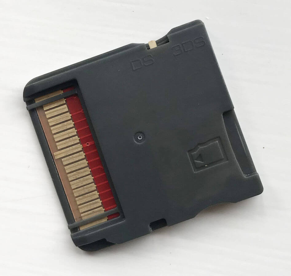
At this point, there was only one question left: How could users install boot9strap?
Well, the team didn’t stop there. By taking a look at their recent Boot ROM dumps, they found an interesting routine: During boot, Boot9 will query if a specific key combination is pressed and the lid is closed. If so, Boot9 will redirect execution to the inserted Nintendo DS card (with full privileges).
Thus, ntrboot came to fruition: Flash a sighax-signed payload into a Nintendo DS flashcard, use a magnet to simulate a closed shell and press the required key combination. Instant Boot9 privileges.
If this wasn’t enough, Nintendo couldn’t fix any of these vulnerabilities through software updates, as they’re hardwired into the Boot ROM. A possible solution would’ve been to ship new hardware revisions, yet, none ever appeared.
The remaining years (2018-present)
Now that the homebrew community has achieved its magnum opus, the remaining years of the Nintendo 3DS will only see the streamlining of hacking methods, all of which share the same objective: Install boot9strap.
By this point in time, there were many exploits in the wild: ‘SoundHax’, ‘Safehax’, ‘Browserhax’… too many to mention here. For the curious, 3DBrew provides a comprehensive list [147].
To give you an idea of how elegant exploitation became by 2023, let me show you a common method users relied on and didn’t require extra hardware. This process was called ‘seedminer + BannerBomb3’ and combined the following vulnerabilities, the majority of them authored by zoogie:
- seedminer: User data installed in the 3DS’ SD card is encrypted using AES-128-CTR. Its key is constructed from other keys found in a file called
movable.sed(console-unique, stored in NAND). Well, it was discovered that this file can be re-constructed by using the console’s Friend Code, subdirectory names in the SD card (generated by the console) and short-term brute-forcing. Once extracted, the keys allowed to tamper with DSiWare data in the SD card. - BannerBomb3: An exploit that overflows the stack of the Settings app while it tries to parse the banner of an installed DSiWare title [148]. Combined with seedminer, this serves as an entry-level exploit with Kernel11 privileges.
- Now, how to take advantage of BannerBomb3 (i.e. which payload to use) depended on the tutorial the user was following at the time. For simplicity purposes, there were two routes:
The Safe Mode route
This route consisted of exploiting SAFE_FIRM and was described in earlier tutorials:
- unSAFE_MODE: Users can boot into Safe Mode by pressing a combination of buttons during the console’s boot, the alternative firmware then enables the user to perform a system update, which is useful for repairing the console. Well, zoogie discovered that the proxy settings can be overflowed [149]. Hence, providing userland execution within Safe Mode.
- safehax: a port of ‘firmlaunch-hax’ to work under SAFE_FIRM. Nintendo originally patched it with system update
9.5.0released in February 2015 [150]. Yet, SAFE_FIRM is an immutable replica of the factory firmware, and thus it features old exploits NATIVE_FIRM once enjoyed.- firmlaunch-hax: When the firmware is booting, the ARM9 stores the firmware’s header in FCRAM for verifying and then parsing. With the help of a race condition, execution can take control of the ARM9, so the boot9strap installer can be launched. Nintendo fixed this by keeping the header in ARM9 RAM instead, although this stayed unpatched on SAFE_FIRM.
The HOME Menu route
Sometime later, a new route was proposed by new tutorials. This exploited the HOME Menu with a new Menuhax-style hack:
- menuhax67: The screen brightness configuration value can be overflown [151], leading to userland control from the HOME Menu.
- nimdsphax: An modern exploit chain combining ‘ctr-httpwn’, ‘nimhax’ and ‘dsp pwn’ [152].
- ctr-httpwn by yellows8: The HTTP service used for network connections can be controlled by overriding its heap memory (using the old GPU DMA exploit) [153].
- nimhax by luigoalma: Uses ctr-httpwn to escalate and take over the services that control the user file system, console configuration and application management [154].
- dsp pwn by luigoalma: Uses nimhax to take control of the DSP, which in turn uses the GPU’s DMA to override the Kernel9 memory space. Thus, obtaining ARM9 privileges.
Post-2023 and conclusions
Be as it may, at the time of this writing, Nintendo hasn’t quite surrendered to the cat-and-mouse game. In May 2023, system update 11.17.0 patched BannerBomb3, nullifying one of the last entry points that didn’t require additional materials [155]. This means users will now need to either obtain a legitimate 3DS game (which can then be exploited), an ntrboot-compatible DS flashcard; or wait for a WebKit exploit (there’s one only left for the New 3DS browser [156]).
That’s all folks
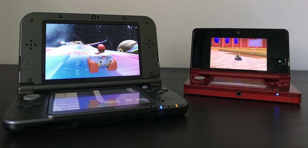
Phew, that was another one of those long articles. I’m glad you managed to keep up and reach the end!
If you are curious, this article took me almost a year to finish, mainly due to a combination of multiple factors, but the important thing is that I ultimately managed to complete it.
Looking back, it’s hard to admit this console didn’t enjoy the same degree of success as the Nintendo DS. Considering all of its offerings analysed here, I think many external factors hindered its marketing. For starters, the timing was unfortunate and the price tag wasn’t exactly tempting. From my perspective, back when it launched in 2011, the ‘08 financial crisis was hitting hard (I was living in Spain back then), so the Nintendo 3DS wasn’t exactly on adults’ (and kids’) priorities. I eventually got mine in 2018, by then living in the UK.
In any case, I want to thank the #ReSwitched and #Godmode9 for spotting lots of mistakes in my initial drafts. This has been the most intricate console I’ve written about (to this date!), nevertheless, I’m very grateful to find communities willing to help out.
Until next time!
Rodrigo


