Supporting imagery
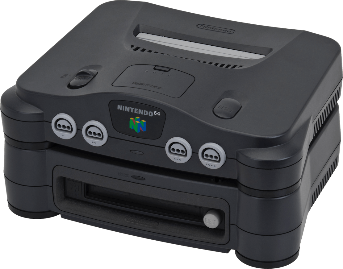
Models

Released on 23/06/1996 in Japan, 29/09/1996 in America and 01/03/1997 in Europe
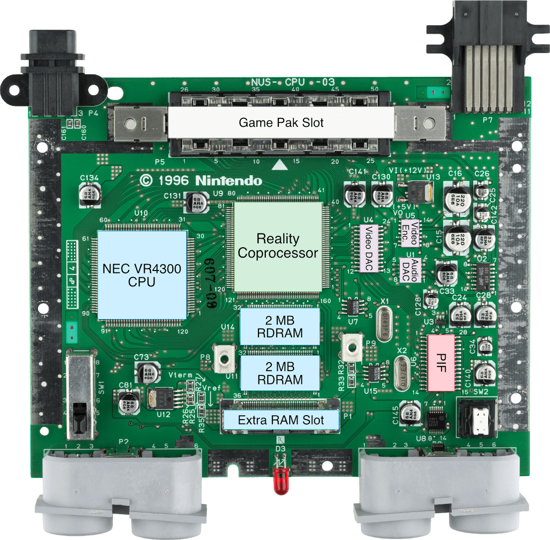
Motherboard
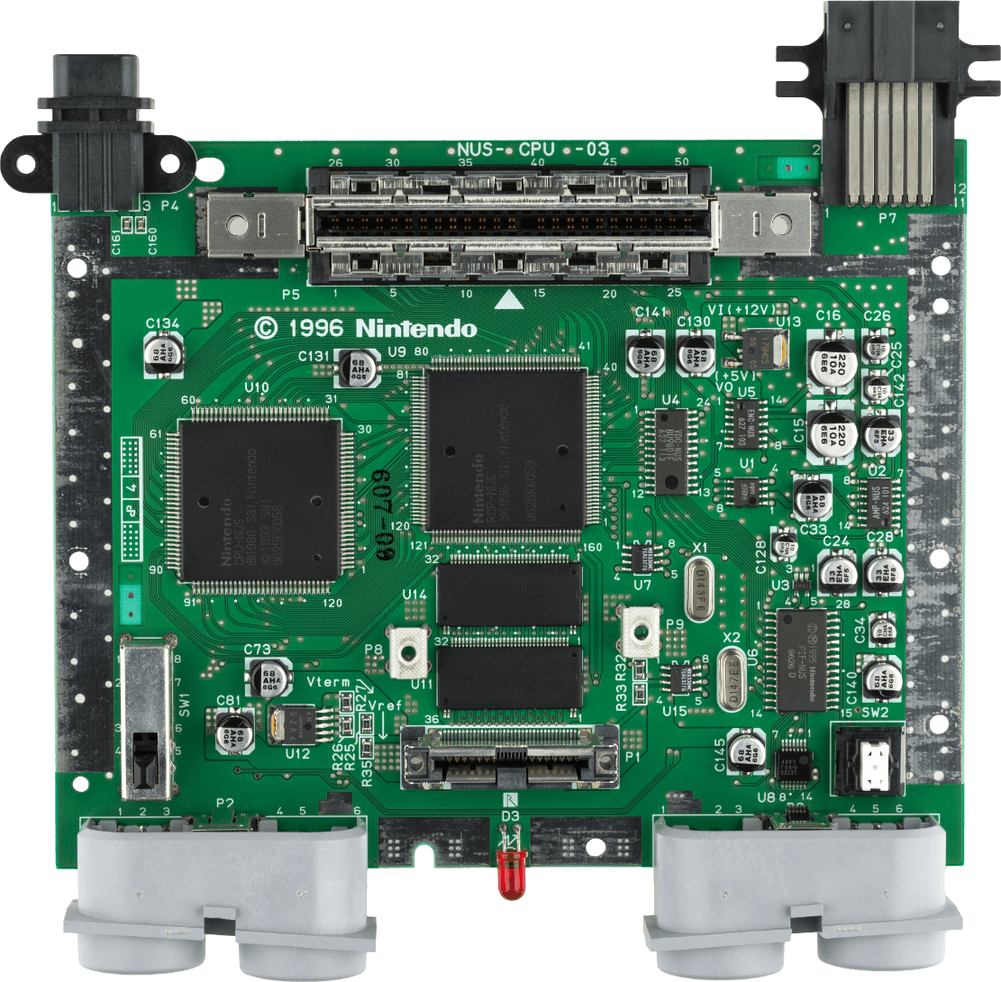
Showing revision 'NUS-CPU-03'.
Later ones reduced the number of chips required for AV encoding.
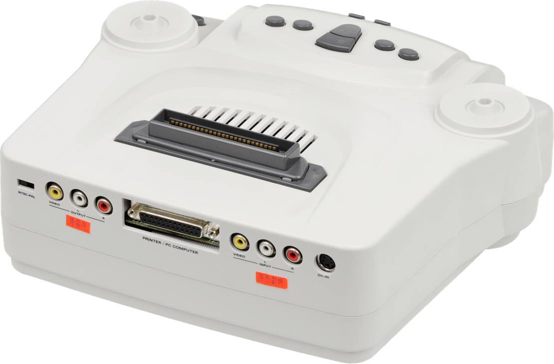
Disk Drive connector is found on the back
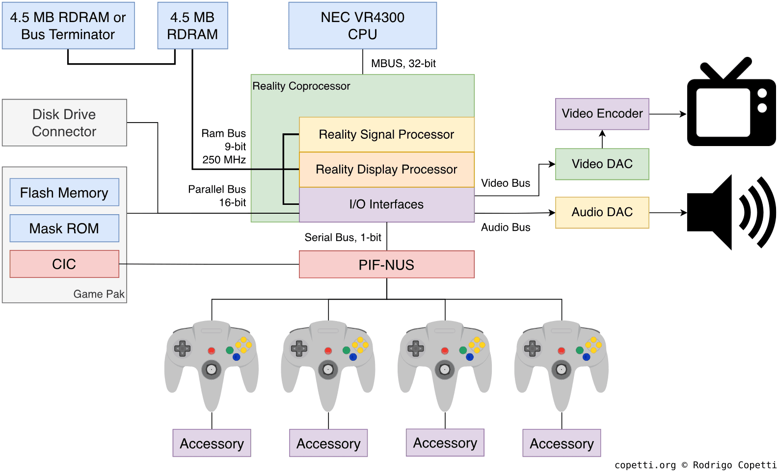
Diagram
A quick introduction
Nintendo’s goal was to give players the best possible graphics. For this, it partnered with one of the biggest names in computer graphics to produce the ultimate graphics chip.
The result was a sleek console for the family… and a 500-page manual for the developer.
Don’t worry, I promise this article won’t be that long… Enjoy!
CPU
The origins of the Nintendo 64’s main processor trace back to the MIPS R4000, MIPS’ new avant-garde CPU. Released in 1991, the R4000’s most apparent novelty was the inclusion of 64-bit capabilities, which resulted from widening the buses, registers and computation units to manipulate 64-bit values with efficiency. Developers, on the other hand, accessed these capabilities through the new MIPS III instruction set. All in all, the R4000 enabled new applications to manipulate larger chunks of data without consuming extra cycles.
For their next-generation console, Nintendo looked into bringing industrial hardware into the home. Unlike Sony, who owned an array of in-house components and only needed a MIPS second-source, Nintendo formed a direct partnership with the owners of MIPS (and numerous graphics workstations) to co-design their entire ecosystem. That company was Silicon Graphics Incorporated (SGI).
Back at SGI’s headquarters, the R4000 was an expensive product (priced at around $400 [1]), which made it unfeasible for a video game console. Still, Nintendo didn’t want to give up on their state-of-the-art ambitions, so they opted for a low-end variant called R4300i, which NEC was able to second-source.
In the end, Nintendo and SGI settled on the NEC VR4300 clocked at 93.75 MHz [2]. This is a binary-compatible version of the MIPS R4300i that features [3]:
- Two modes of operation:
- 32-bit mode: Traditional mode in which the CPU behaves as a MIPS II-compatible processor. There’s nothing special about this mode except that all new functions are locked out.
- 64-bit mode: ‘Native’ mode where all 64-bit extensions are available. It’s also binary-compatible with 32-bit applications.
- 32 general-purpose registers: These are 32 bits wide in 32-bit mode, and 64 bits wide in 64-bit mode.
- The MIPS III ISA: A RISC instruction set that builds on MIPS II. It introduces new opcodes for computing 64-bit words (called ‘doublewords’). Finally, instructions are always 32-bit long, regardless of mode.
- It’s worth mentioning that, starting with MIPS II, load delay slots became optional. Instead, the hardware can automatically interlock/stall the pipeline to prevent data hazards. This is an interesting contradiction to MIPS’ initials!
- Weirdly, branch delay slots still persist, but there are new branch instructions that can discard the delay slot. Although these were removed in later revisions of the instruction set [4].
- An internal 64-bit bus connected to an external 32-bit data bus: While doublewords operations don’t degrade performance when operated internally, moving 64-bit data across the system incurs extra cycles.
- This is one of the cutbacks of the R4300i variant (the R4000 features a full 64-bit data bus).
- 32-bit address bus: Capable of addressing up to 4 GB of physical memory.
- Five-stage pipeline: Up to five instructions can be allocated for execution (a detailed explanation can be found in a previous article).
- 24 KB of L1 cache: Partitioned into 16 KB for instructions and 8 KB for data.
The package also includes an internal Floating-Point Unit (FPU). The VR4300 designates it as a co-processor (CP1), however, the unit is fitted adjacent to the ALU and accessed solely via the ALU pipeline, meaning there’s no co-processing per se. On the other side, the FPU still houses a dedicated register file and speeds up operations involving 64-bit and 32-bit floating-point numbers. Finally, this unit adheres to the IEEE 754 standard.
Simplified memory access
The way RAM is assembled follows the Unified Memory Architecture (UMA), wherein all available RAM is centralised in one place only, and any component requiring RAM access draws from this shared location. The unit arbitrating its access is, in this case, the graphics chip.
The reason for choosing this design comes down to manufacturing costs. At the same time, if not managed properly, it also increments access contention.
No DMA controller?
As a consequence of the unified memory architecture, the CPU no longer has direct access to RAM. Thus, the graphics chip provides the required Direct Memory Access (DMA) functionality as well.
Memory design
Apart from the UMA, the structure of RAM is a little bit complicated, so I’ll try to keep it simple. Here it goes…
The system physically contains 4.5 MB of RAM; however, it’s connected using a 9-bit data bus, where the 9th bit is reserved for the GPU (I explain more in the ‘Graphics’ section). As a consequence, every component except the GPU will only find up to 4 MB.
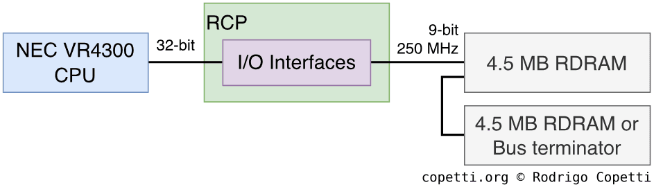
The type of RAM fitted to the board is called Rambus DRAM (RDRAM) [5]. This was just another design that competed with ‘Synchronous DRAM’ (SDRAM) to become the next standard. RDRAM is connected using a fast serial architecture (where memory modules are chained in sequence), while SDRAM employs a slower parallel connection (wiring all modules directly to the memory controller). Each came with its own advantages and disadvantages, both technical and commercial. Nevertheless, it’s worth pointing out that although SDRAM ultimately triumphed, RDRAM continued to appear in later console generations, each introducing a new revision of the protocol.
Finally, the Nintendo 64 implemented the Base RDRAM variant [6] - the very first revision of the protocol.
Latency and speed
While RDRAM installations required less wiring and enjoyed greater clock speeds than SDRAM, access latency increased proportionally with the number of banks installed [7]. In the case of the Nintendo 64, the delay between initiating a memory transaction to finding the value in cache was significant - around 640 ns [8]. Engineers tried to offset this by applying a high clock speed of 250 MHz (approximately 2.6 times faster than the CPU) to the memory banks. This way, Nintendo claimed that RDRAM could deliver high-speed data transfers of up to 500 MB/sec when reading or writing consecutive data [9].
As a side note, Nintendo chose NEC’s uPD488170L memory banks for the N64’s motherboard [10]. These chips implement a technology known as ‘Rambus Signaling Logic’ - an umbrella term used to promote many advancements, one of which doubles the transfer rate [11]. This may explain why some sources cite the ‘effective’ memory rate as 500 MHz.
Leaving room for improvement
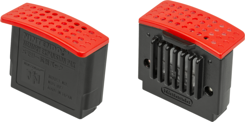
Interestingly, the amount of available RAM on this console can be expanded by installing the Expansion Pak accessory - a peculiar box that adds another 4.5 MB. While this accessory remained optional for some games (and the majority didn’t make use of it), certain titles such as Donkey Kong 64 and The Legend of Zelda: Majora’s Mask were designed with the expansion as a requirement, and would display an error screen if it was not present.
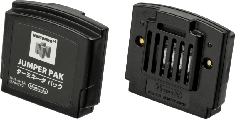
Due to its end-to-end design, RDRAM must be properly terminated; otherwise, signals would bounce back and forth along the bus (a common phenomenon known as reflection). Rambus mitigated this by requiring PC users to install memory modules in pairs and to fill all unused slots with ‘Continuity RIMM’ (CRIMM) modules, which acted as terminators. For this console, however, Nintendo shipped a terminator called Jumper Pak, which came fitted in place of the Expansion Pak. The Jumper Pak housed only enough capacitors and resistors to match the bus’s impedance [14], thereby reducing reflection. It also served to close the loop in the serial chain [15].
Now, you may ask, what would happen if you switched on the console without any Pak installed? Well, the onboard memory chips won’t be functional, so the boot sequence will fail and nothing will come out of the video signal.
Memory management
The VR4300 includes another coprocessor known as the System Control Coprocessor (CP0), which is composed of a Memory Management Unit (MMU) and a Translation Lookaside Buffer (TLB). The MMU governs how memory is organised and cached.
Although the CPU is capable of addressing up to 4 GB worth of memory, the Nintendo 64 contains far less, even after considering memory-mapped I/O. For that reason, the MMU provides efficient uses for addressing limited memory, including a virtual memory map in which physical memory is mirrored multiple times. Consequently, memory locations are treated as virtual addresses (as opposed to ‘physical addresses’). Furthermore, this layout is enhanced by the TLB, which enables developers to define custom memory maps in some mirrors without adding (significant) performance penalties.
At first glance, all of this may seem redundant. However, each mirror (called segment) is connected to distinct circuitry (e.g. L1 cache, physical RAM, or TLB-mapped regions), allowing developers to optimise usage by selecting the most appropriate segment depending on the needs [16].
Some segments were designed to distinguish between ‘kernel’ and ‘user’ locations for security purposes. Nevertheless, the N64 always operates in ‘kernel’ mode, making the ‘non-TLB kernel cached’ segment (called ‘KSEG0’) the most commonly used for games.
Finally, the MMU can also work in 64-bit mode, where memory addresses are 40 bits long. This extends the virtual address space to approximately 1 TB worth of addresses… but I don’t think the Nintendo 64 will ever take advantage of this!
Graphics
What you see on screen is produced by a large chip designed by Silicon Graphics called Reality Co-Processor (RCP), which runs at 62.5 MHz [17]. This package contains a lot of circuitry, so don’t worry if you find it difficult to follow - the graphics subsystem has a very complex architecture!
This design is based on the philosophy that the GPU should not be a ‘mere’ rasteriser like the competition. Instead, it should also be capable of accelerating geometry calculations (offloading work from the CPU), and for that, more circuitry is needed.
Architecture
The Reality Co-Processor is divided into three main modules, two of which are dedicated to graphics processing:
Reality Signal Processor
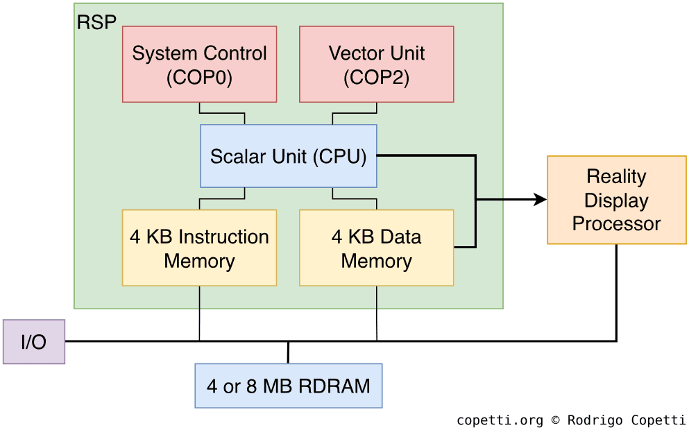
Also known as RSP, the Reality Signal Processor is a CPU package composed of [18]:
- The Scalar Unit: Another cut-down derivative of the MIPS R4000. This time, it only implements a subset of the MIPS III ISA, and therefore lacks many general-purpose functions, including interrupts, the 64-bit extension, multiplication, and division.
- The Vector Unit: A co-processor that performs vector operations with 32 128-bit registers. Each register is sliced into eight parts to operate eight 16-bit vectors at once (similar to SIMD instructions in conventional CPUs). As you can see, this component does the heavy lifting for the Scalar Unit (while also working concurrently).
- The System Control: Another co-processor that provides DMA functionality and controls its neighbouring module, the RDP (explained in the next section).
To operate the RSP, the CPU stores a series of commands called Display list in RAM, along with the data to be manipulated. The RSP then reads the list and performs the required operations on it. Available functions include geometry transformations (such as perspective projection), clipping, and lighting.
This may seem straightforward, but how does it perform these operations? Well, here’s the interesting part: unlike its competitors (the PlayStation and Sega Saturn), the geometry engine is not hard-wired. Instead, the RSP contains some memory (4 KB for instructions and 4 KB for data) to store microcode [19]: A small program, with no more than 1000 instructions, that implements the graphics pipeline. In other words, it tells the Scalar Unit how to process the graphics data. The microcode is fed by the main CPU at runtime.
Nintendo provided multiple microcodes to choose from and, similar to the SNES’ background modes, each one balances system resources differently [20].
The resulting data is transmitted either via a dedicated bus called XBUS or through main RAM. Over the console’s lifetime, this choice fluctuated due to memory constraints: the XBUS path was faster but required additional buffers in the RSP’s internal memory to hold (and transfer) the new data. To give you an idea, early microcode programs like Fast3D offered both options. However, the later and faster F3DEX focused entirely on main RAM. Finally, its successor, F3DEX2, reintroduced XBUS support after sorting out memory usage.
Reality Display Processor
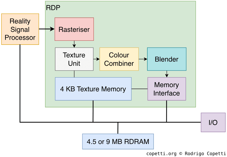
After the RSP finishes processing the data, it will start sending rasterisation commands to the next module - the Reality Display Processor (RDP) - to draw the frame.
The RDP is another processor (this time with fixed functionality) that includes multiple engines to rasterise vectors, map textures onto polygons, mix colours, and compose the new frame.
It can process either triangles or rectangles as primitives, the latter being useful for drawing sprites. The RDP’s rasterisation pipeline contains the following blocks [21]:
- A Rasteriser: Converts primitives (made of vertices) into pixels.
- A Texture Unit: Processes textures using 4 KB of dedicated memory (called ‘TMEM’), allowing up to eight tiles to be used for texturing. It can perform the following operations on them:
- Bilinear filtering: Maps the selected 2D texture onto the 3D shape and smooths it to avoid pixelated areas (caused by oversampling).
- A ‘complete’ filter would require four points to carry out the interpolation; however, this console uses only three (triangular interpolation), resulting in some anomalies. Thus, certain textures have to be ‘adapted’ beforehand.
- Mip-Mapping: Automatically selects a scaled-down version of the texture depending on its level of detail. This avoids computing large textures that are seen far from the camera and prevents aliasing (the result of undersampling).
- If enabled, the RDP maps textures using trilinear filtering instead. This new algorithm also interpolates between mipmaps to soften abrupt changes between the levels of detail.
- Perspective correction: The chosen algorithm for mapping textures onto triangles. Unlike other inverse-mapping algorithms, this one accounts for the depth value of each primitive, achieving more faithful results.
- Bilinear filtering: Maps the selected 2D texture onto the 3D shape and smooths it to avoid pixelated areas (caused by oversampling).
- A Colour Combiner: Mixes and interpolates multiple layers of colours. As the next-generation color math unit, it performs addition, multiplication, and subtraction of colour values.
- A Blender: Mixes pixels with the current frame buffer to apply translucency, anti-aliasing, fog, and dithering. It also performs z-buffering, which I explain more later on.
- A Memory Interface: Used by the previous blocks to read from and write to the current frame buffer in RAM and/or populate TMEM.
The RDP provides four operating modes, each of which combines these blocks differently to optimise specific tasks.
Since this module constantly updates the frame buffer, it interacts with main RAM in a unique way. Remember the unusual 9-bit ? The ninth bit is used as metadata for frame buffer-related calculations (i.e. z-buffering and antialiasing) and is only understood by the Memory Interface.
Remaining steps
The resulting frame must be sent to the Video Encoder to be displayed on-screen. DMA and the Video Interface component are essential to accomplish this.
The theoretical maximum capabilities of the output frame are a 24-bit colour depth (16.8 million colours) and a resolution of 640x480 pixels (or 720x576 in the PAL region) [22]. I mention ‘theoretical’ because using the maximum capabilities can be resource-hungry, so programmers often opt for lower specifications to free up enough resources for other services.
Quick demo
Let’s put all the previous explanations into perspective, for that, I will use Nintendo’s Super Mario 64 as a case study to show, in a nutshell, how a basic frame is composed. Just bear in mind that, in practice, however, games may employ additional buffers to compose richer frames.
Vertex Processing
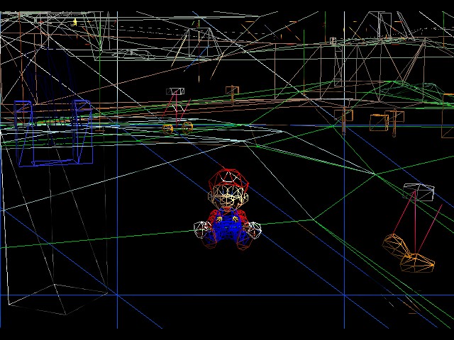
Initially, materials such as 3D models are located in the cartridge ROM. However, to keep a steady bandwidth, we need to copy them to RAM first. In some cases, the data is pre-compressed within the cartridge, requiring the CPU to decompress it before use.
Once that’s done, it’s time to build a scene using our models. The CPU could carry out the entire graphics pipeline by itself, but that takes ages, so many tasks are offloaded to the RCP. The CPU will instead send orders to the RCP, this is done by carrying out these steps:
- Compose the Display Lists that contain the operations to be executed by the RSP, and store them in RAM. The structure of Display Lists is dictated by the choice of microcode [23].
- Point the RSP to the location of the Display Lists.
- Upload the chosen microcode to the RSP, kickstarting the Scalar Unit.
Afterwards, the RSP begins working on the first batch of tasks. The result is then passed to the RDP in the form of rasterisation commands.
Pixel processing
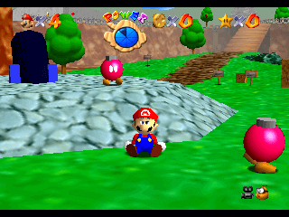
So far, we’ve managed to process our data and apply some effects, but we still need to:
- Rasterise vectors, apply textures and other effects.
- Display the frame buffer.
As you might expect, these tasks are performed by the RDP. Additionally, to make this work, textures must be transferred into the 4 KB of Texture Memory using DMA.
Unlike the previous processor, the RDP’s pipeline is fixed, but we can select the optimal mode of operation based on workload, performance and specific tasks needed. For instance, commanding the RDP to render a single texture is faster than combining two.
Once the RDP finishes processing the data, it writes the final bitmap to the frame buffer area in RAM. Afterwards, the CPU must transfer the new frame to the Video Interface (VI), preferably using DMA. The VI, in turn, sends it to the Video Encoder for display [24].
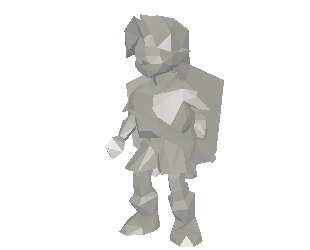
Designs
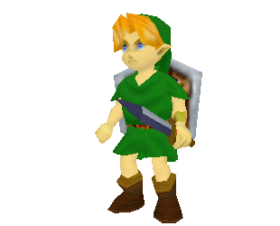
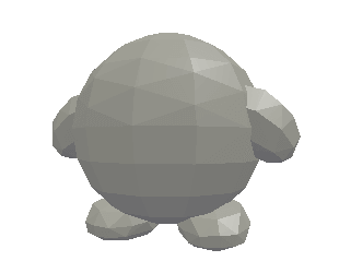
Here are some examples of classic 2D characters from the Super Nintendo that were redesigned for the 3D era. Notice the texture detail when compared with models from other consoles of the same generation.

 Interactive model available in the modern edition
704 triangles.

 Interactive model available in the modern edition
516 triangles.
Modern visible surface determination
If you’ve read about the preceding consoles, you’ll have come across the never-ending problem of visibility of surfaces, and by now may think polygon sorting is the only way out of this. Well, for the first time in this series, the graphics chip features a hardware-based approach called Z-buffering. In a nutshell, the RDP allocates an extra buffer (called Z-buffer) in memory. This has the same dimensions as a frame buffer, but instead of storing RGB values, each entry contains the depth (Z-value) of the nearest pixel relative to the camera.
After the RDP rasterises the vectors, the z-value of the new pixels are compared against the corresponding value in the z-buffer. If the new pixel has a smaller z-value, it means the new pixel is positioned in front of the previous one, so it is applied to the frame buffer and the z-buffer is also updated. Otherwise, the pixel is discarded.
Overall, this is a hugely welcome addition: programmers no longer need to worry about implementing software-based polygon sorting methods, which drain significant CPU resources. However, the z-buffer does not prevent feeding unnecessary geometry (whether discarded or overdrawn, both wasting resources). For this, game engines may choose to include an occlusion culling algorithm to discard unseen geometry as early as possible.
Secrets and limitations
SGI clearly invested a lot of technology into this system. Nevertheless, the Nintendo 64 was a console intended for the home market and, as such, needed to keep its cost down. Some tough compromises resulted in difficult challenges for programmers:
Pipeline Stalls
The deprecation of load delay slots in MIPS II, in favour of automatic pipeline stalls, had the benefit of alleviating the need for filler instructions. However, this breakaway from MIPS’ core philosophy also exposed new bottlenecks. Due to the large number of components and operations in the graphics pipeline, the RCP became highly susceptible to excessive stalls: an undesirable situation in which sub-components remain idle for considerable periods, as the required data is delayed at the back of the pipeline.
This invariably results in performance degradation, and it is the programmer’s job to avoid. Although, to help mitigate this, MIPS CPUs had long provided pipeline bypassing, a mechanism that enables similar instructions to execute at a faster rate by bypassing some execution stages that can be skipped [25].
For example, if the CPU has to compute sequential ADD instructions that are dependent on each other, there’s no need to write the result back to a register and then read it again after each operation. Instead, the CPU can forward the values within the datapath and perform the write-back only after the last ADD has been completed.
Texture memory
The RDP relies on 4 KB of Texture Memory (TMEM) as a single source for loading textures. Unfortunately, 4 KB proved to be insufficient for high-resolution textures. Furthermore, when mipmapping is activated, the available memory is reduced to half.
As a result, some games used solid colours with Gouraud shading (Super Mario 64 being a notable example), while others relied on pre-computed textures (particularly, where multiple layers had to be combined).
The universal video out
Nintendo carried on using the ‘universal’ Multi Out port from its predecessor, bad news is that it no longer carries the RGB signal! It looks to me like another cost-saving measure, given that RGB wasn’t widely adopted in the previous console.
The good news is that, on early revisions of the Nintendo 64, the three RGB lines can still be restored by soldering some cables and fitting an inexpensive signal amplifier. This is possible because the video Digital-to-Analogue Converter (DAC) still transmits an RGB signal to the video encoder [26]. However, later motherboard revisions combined both chips, so the only remaining option is to bypass the video DAC and encoder altogether with custom circuitry that exposes RGB signals.
Audio
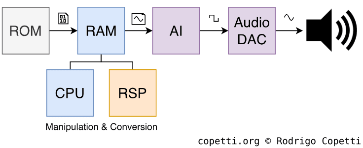
Before we go into the details, let’s define the two endpoints of the N64’s audio subsystem:
- Our starting point is the cartridge ROM, which contains data that only the CPU can interpret.
- The ending point is the Digital-to-Analog Converter (DAC), which only understands waveform data [27].
Now, how do we connect both ends? Consoles normally include a dedicated audio chip that does the work for us. Unfortunately, the Nintendo 64 doesn’t have a dedicated chip, so this task is distributed across these components:
- The main CPU: Transfers the audio data from the game’s ROM to RAM, then composes Audio Lists to be handled by the RSP.
- The RSP: Using additional microcode, it interprets the audio lists previously stored in RAM and performs the required operations on the audio data, which can include:
- Decompressing ADPCM samples and applying effects.
- Sequencing and mixing MIDI data using audio banks stored in RAM.
The resulting data is, as expected, waveform data. This is then sent to the Audio Interface (AI) block, which transfers it to the digital-to-analogue converter [28]. Being a stereo system, the resulting waveform contains two channels, each with 16-bit resolution.
The repertoire
Time to check out the soundtracks made for the N64. There are too many (good ones) to mention in this article, so here are some that caught my attention:
The music of this game is tied to its daunted atmosphere.
This game has a nice and unique house-based soundtrack.
Secrets and limitations
Because of this design, the constraints are dictated by the overall workload:
- The sampling rate can be up to 44.1 kHz, but using the top rate steals too many CPU cycles.
- There’s no strict limit on the number of channels; it all depends on how much the RSP is capable of mixing (often around 16-24 channels when processing ADPCM, or approximately 100 with PCM).
- Memory is another concern. While competitors relied on larger media (i.e. CD-ROM) and dedicated audio memory, Nintendo 64 cartridges hold much less data (let alone music data) and must share main memory with other components.
For these reasons, players may notice that N64 ports feature lower-quality music or repeated scores. A common workaround is to implement a music sequencer that generates samples at runtime using a pre-populated set of sounds (resembling MIDI music).
Operating System
Similar to the PS1 and Saturn, N64 games are written for bare metal. However, there are no BIOS routines available to simplify hardware operations. As a substitute, games embed a small operating system that provides a fair amount of abstraction to efficiently manage the CPU, GPU, and I/O.
This is not the conventional desktop OS that we may imagine at first, it’s just a microkernel with the smallest possible footprint that offers the following functionality [29]:
- Multithreading using message passing.
- Scheduling and preemption.
- Simplified register and I/O access.
All in all, these functions are critical for coordinating audio, video, and game logic tasks - all of which need to work concurrently - in an efficient manner.
The kernel is automatically embedded when using Nintendo’s libraries. Additionally, if programmers decide not to include part of the library set, the corresponding portion of the kernel is stripped to avoid wasting cartridge space.
Boot process
Unlike previous cartridge-based systems, the Nintendo 64 follows a sophisticated boot process to prepare all of its hardware before the actual game runs. This process begins as soon as the user powers on the console and is very similar to its CD-based contemporaries bundling a BIOS or IPL.
These routines are also referred to as Initial Program Loader (IPL) and work as follows [30] [31]:
- The user turns on the console.
- The PIF-NUS (a separate chip on the motherboard) subdues the main CPU into an infinite reset until it validates the CIC chip found in the game cartridge.
- The PIF-NUS and the CIC chip are explained further in the I/O and anti-piracy sections, respectively.
- If the verification process finishes successfully, the CPU starts execution at
0xBFC00000. This address points to an internal ROM within PIF-NUS, specifically the first boot stage called IPL1. - IPL1 initialises part of the hardware (CPU registers, the parallel interface, and the RCP), then copies the next stage (IPL2) from the internal ROM to the RSP’s memory for faster execution. It then redirects execution there.
- IPL2 copies the first four bytes of the game ROM into the RSP’s memory. This is used to adjust the ROM bus timings. Afterwards, it copies another 4 KB of the ROM header and sends a checksum of it to the PIF-NUS, which verifies the checksum using the cartridge’s CIC chip. If the verification fails, the PIF-NUS interrupts the CPU indefinitely. Otherwise, the CPU continues execution on those 4 KB, which contain the next boot stage, called IPL3.
- IPL3 initialises RDRAM, the CPU cache, and the Expansion Pak (if present). Afterwards, it copies 1 MB of game ROM into RDRAM, computes its checksum, and compares it against a precomputed value stored in the ROM header. Finally, the CPU jumps to the game code in RDRAM.
As IPL3 resides within the game cartridge, not every game includes the same code. Additionally, the IPL3 checksum stored in the CIC is hardcoded [32]. Thus, the CIC chip and IPL3 variants found in the cartridge are bound together and cannot be swapped with different models.
I/O
As you know by now, I/O is not directly connected to the CPU, so the RCP’s third module - which I haven’t mentioned until now - serves as an I/O interface. This block handles communication with the CPU, controllers, game cartridge, and audio/video DACs.
Accessories
In addition to its unorthodox shape, the Nintendo 64 controller includes a connector for plugging in accessories. Notable commercial examples include:
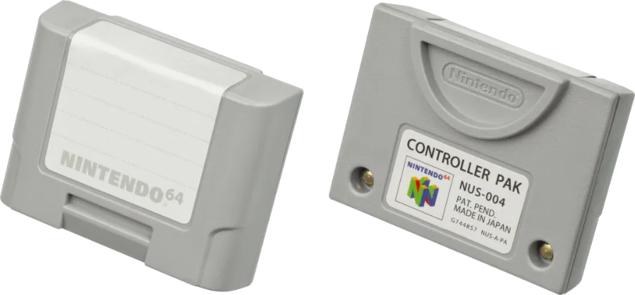
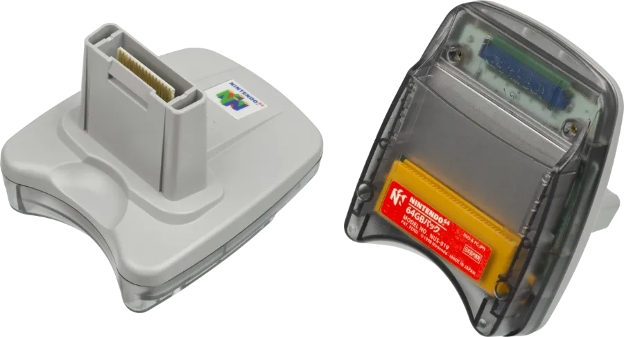
- The Controller Pak: A storage medium, similar to Sony’s Memory Card, used to store save game data and share it across consoles.
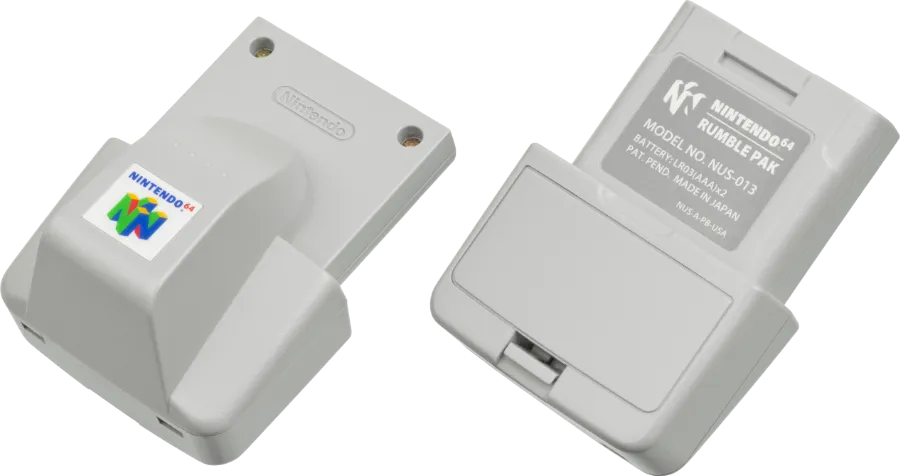
- The Rumble Pak: Contains a small motor that provides haptic feedback, useful for ‘immersing’ the player in supported games.
- The Transfer Pak: Provides a slot to connect a Game Boy or Game Boy Color cartridge (Game Pak). This enabled the possibility to run Game Boy games with the help of an emulator, and/or transfer its content.
All accessories connected to the controller are managed by the PIF-NUS, an obscure block that also handles security. The RCP communicates to the PIF using a serial bus [36].
Games
Nintendo held on to the cartridge medium for storage instead of adopting optical discs. As a consequence, games enjoyed higher bandwidths (an average of 5 MB/sec) while also being more expensive to manufacture. The largest cartridge found in the market had a capacity of 64 MB.
Inside cartridges, manufacturers often included extra memory (in the form of EEPROM, flash, or SRAM backed by battery) to hold save data. However, this became less essential, as certain accessories (like the Controller Pak) provided alternative storage.
Cartridges interface with the RCP using a dedicated 16-bit bus known as the Parallel Bus (PBUS) or ‘Parallel Interface’ (PI) [37].
Source Development Kit
In general, development was mainly done in C and assembly, the latter was often required to achieve better performance.
While we’ve seen this system supports 64-bit operations, the new instructions were rarely used since, in practice, 32-bit instructions happened to execute faster (given that the R4300i/VR4300 comes with a 32-bit data bus).
The libraries in the official SDK feature several layers of abstractions to command the RCP. For example, C structs like the Graphics Binary Interface (GBI) were designed to facilitate the assembly of Display lists [38]. The same applies to audio functions, its struct was called Audio Binary Interface (ABI).
In terms of microcode development, Nintendo provided a set of prewritten microcode programs to choose from. However, if developers wanted to customise them, that would indeed be a challenging task: the Scalar Unit instruction set wasn’t initially documented. Later on, however, Nintendo and SGI changed their stance and released some documentation and tools for microcode programming [39].
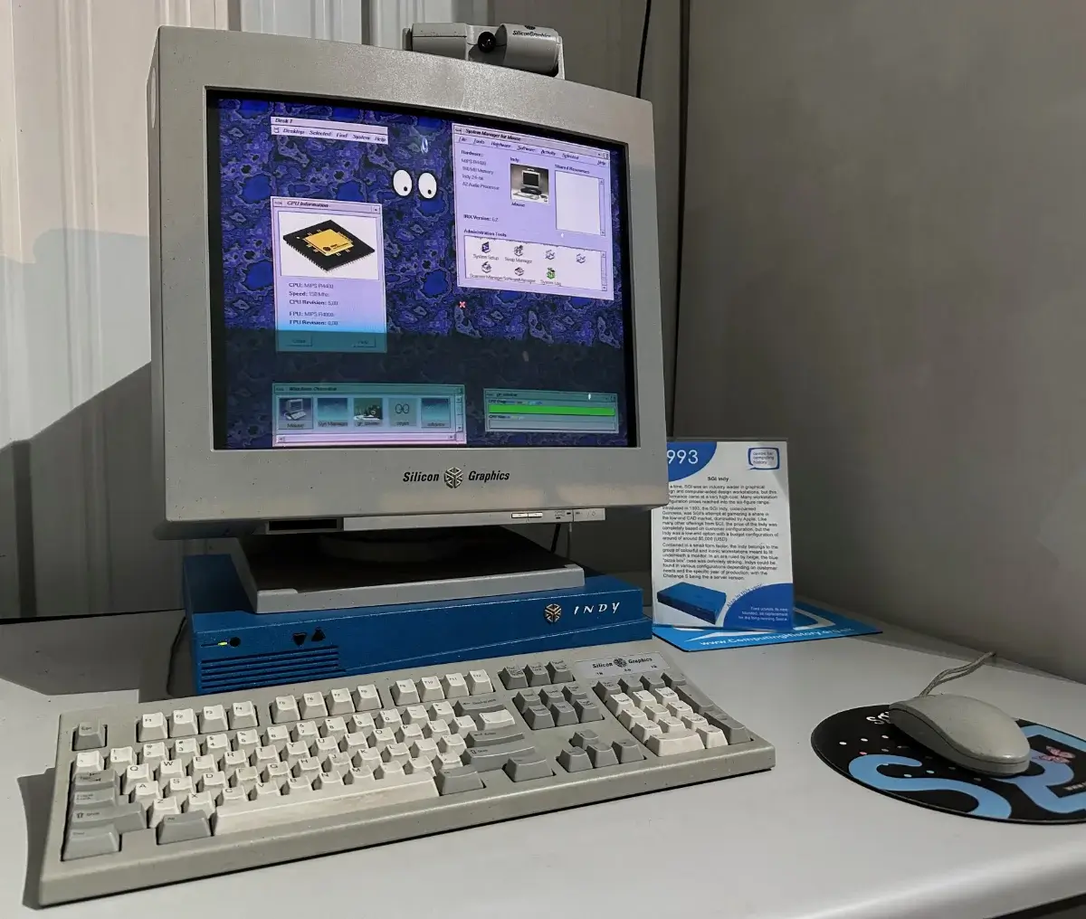
Hardware used for development included workstations supplied by SGI [40], such as Indy machines equipped with an extra daughterboard called U64. This board contained the hardware and I/O of the retail console. Development tools were supplied for Windows-based computers as well [41].
Furthermore, there were third-party tools such as custom cartridges housing a long ribbon cable that connected to the workstation. These cartridges fitted in a retail Nintendo 64 but incorporated internal circuitry to redirect ‘read’ requests from the console to the workstation’s RAM. The deployment and debugging process involved transferring a copy of the game into RAM so that, upon powering the console, it would start reading from there.
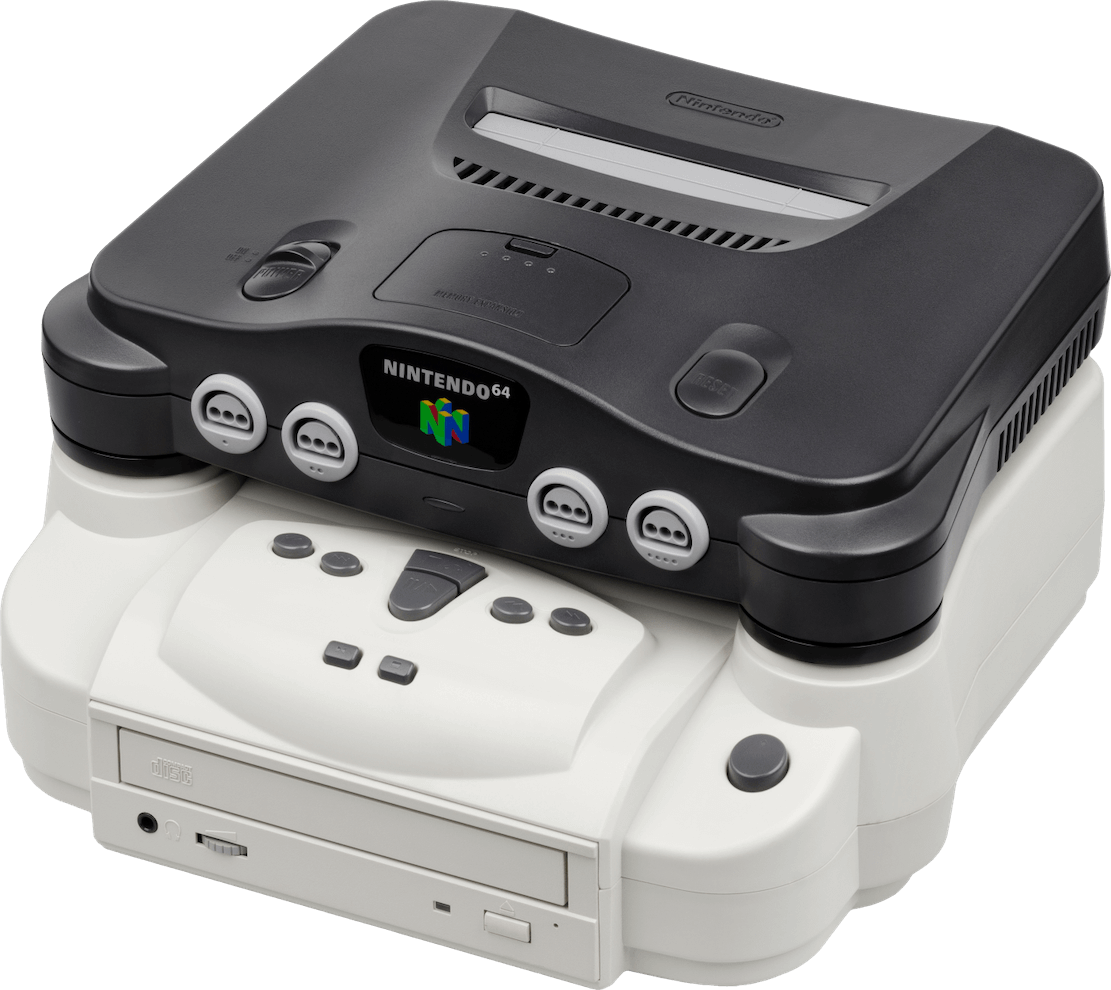
The alternative medium
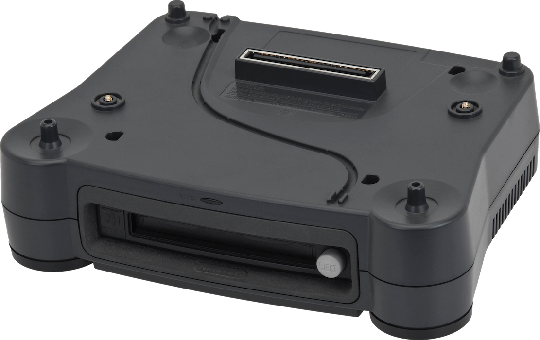
Interestingly, the PBUS branches out to a secondary connector located on the underside of the Nintendo 64’s motherboard. This was intended for the Nintendo 64 Disk Drive (64DD), a peripheral that worked as an ‘extra floor’ beneath the console, housing a proprietary magnetic disk reader. The disks offered up to 64 MB of storage capacity.
Although the 64DD was only released in Japan, it opened the door to an alternative (and cheaper) medium for distributing games.
Released on 01/12/1999 in Japan.
The magnetic medium used by the 64DD is slower than cartridges, with transfer speeds of up to 1 MB/sec - but still faster than 4x CD-ROM readers. The disks are double-sided and operate using Constant Angular Velocity (CAV), like the later miniDVD. The smallest readable area is called a block and corresponds to half of a concentric circle on the disk surface.
Notably, the reader doesn’t include buffer memory, so data is streamed directly into RDRAM for execution. To accommodate the increased memory demands, Nintendo bundled the RAM Expansion Pak with the 64DD. In doing so, it also standardised the extended RAM space, ensuring that all 64DD games could reliably take advantage of the additional memory.
Furthermore, portions of the disk are rewritable to enable save storage. The amount of writable space varies depending on the disk type (Nintendo offered seven types).
On the software side, game data is structured with a filesystem called ‘Multi File System’ (MFS) provided by Nintendo with their SDK [44]. Games could access disk data either through the filesystem or via direct block-level access.
The Disk Drive also houses an internal ROM, known as ‘DDROM’, which stores code executed by the N64 during boot. This code bootstraps the disk and shows the splash animation, effectively adding a new IPL stage on top of the traditional boot process. The ROM also stores fonts (Latin and Kanji) and some sounds.
Anti-piracy / Region Lock
The anti-piracy system is a continuation of the Super Nintendo’s CIC model. As you know, earlier bootleg detection and region locking were enforced by the CIC chip (which was present in every authorised game cartridge) [45]. The Nintendo 64 enhanced this system by assigning specific CIC chip variants to individual games, ensuring that each cartridge was not a counterfeit or contained a CIC clone.
To enforce this, the PIF-NUS conducts checksum verifications both at the startup and during gameplay to supervise the current CIC installed on the cartridge.
If the PIF determines the current cartridge is not valid, it forces the console into a permanent freeze state.
Moving on, region locking was done by slightly altering the shape of the cartridge on a region basis, so users could not physically insert the game on a console from a different region.
Overall, piracy wasn’t a significant concern due to the inherent complexity and cost of replicating cartridges, though game prices were often three times higher than CD-based titles.
Unused ports
As silly as it may seem, Nintendo left one door open: The Disk Drive port.
A few companies reversed-engineered the interface to develop their own peripherals, and some of the resulting products became a concern for piracy.
I guess the most notable case was the Doctor v64, a device resembling the Disk Drive but equipped with a CD-ROM drive instead.
This expansion could back up the contents of the cartridge to a CD, the opposite (reading ROM files from a CD) was also supported.
Emulation
When I was a kid, I used to play some N64 games on a Pentium II machine using an emulator. It wasn’t that bad, though in hindsight, I’m amazed my old computer managed to emulate a complex 64-bit machine - especially given that, among other things, my PC barely had enough RAM to keep the integrated video alive.
The truth is, while reproducing the architecture of this console can be complex, microcode routines will give a hint of what the console is trying to achieve, and since emulators don’t have to be cycle-accurate, they can apply enough optimisations to provide extra performance in exchange for precision [48].
Another reason is the 64-bit instruction set: since games rarely took full advantage of them, emulation performance was hardly affected when running on a 32-bit host computer.
That’s all folks
I have to say, this article may be the longest one I’ve ever written, but hopefully you found it a nice read!
I’ll probably take the following days to tide up some things on the website instead of starting to write the next article.
Until next time!
Rodrigo