Supporting imagery
Model
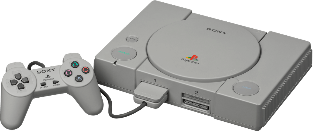
Released on 03/12/1994 in Japan, 09/09/1995 in North America, 29/09/1995 in Europe.
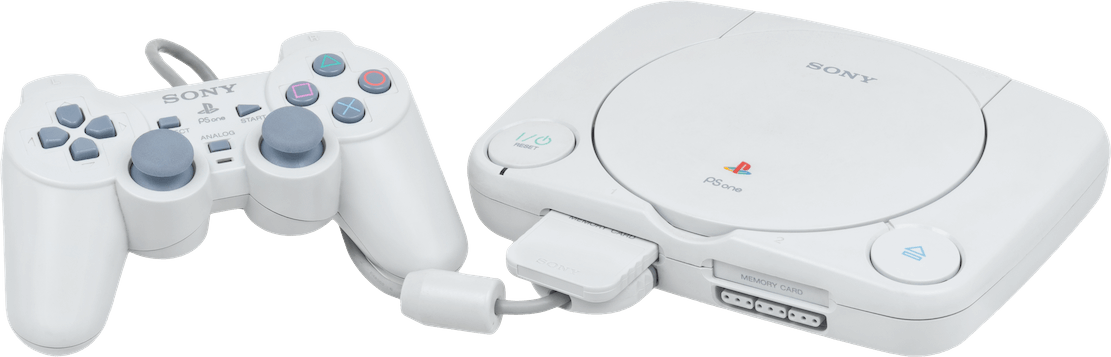
Released on 07/07/2000 in Japan, 19/09/2000 in North America, 29/09/2000 in Europe.
This is what you get after cramming so many custom ICs into a single one.
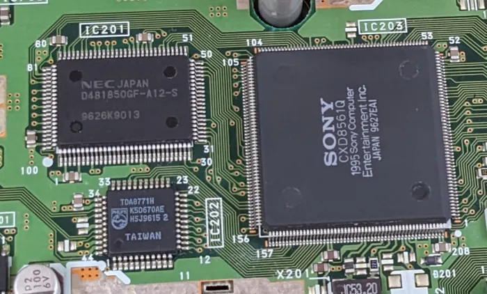
Motherboard
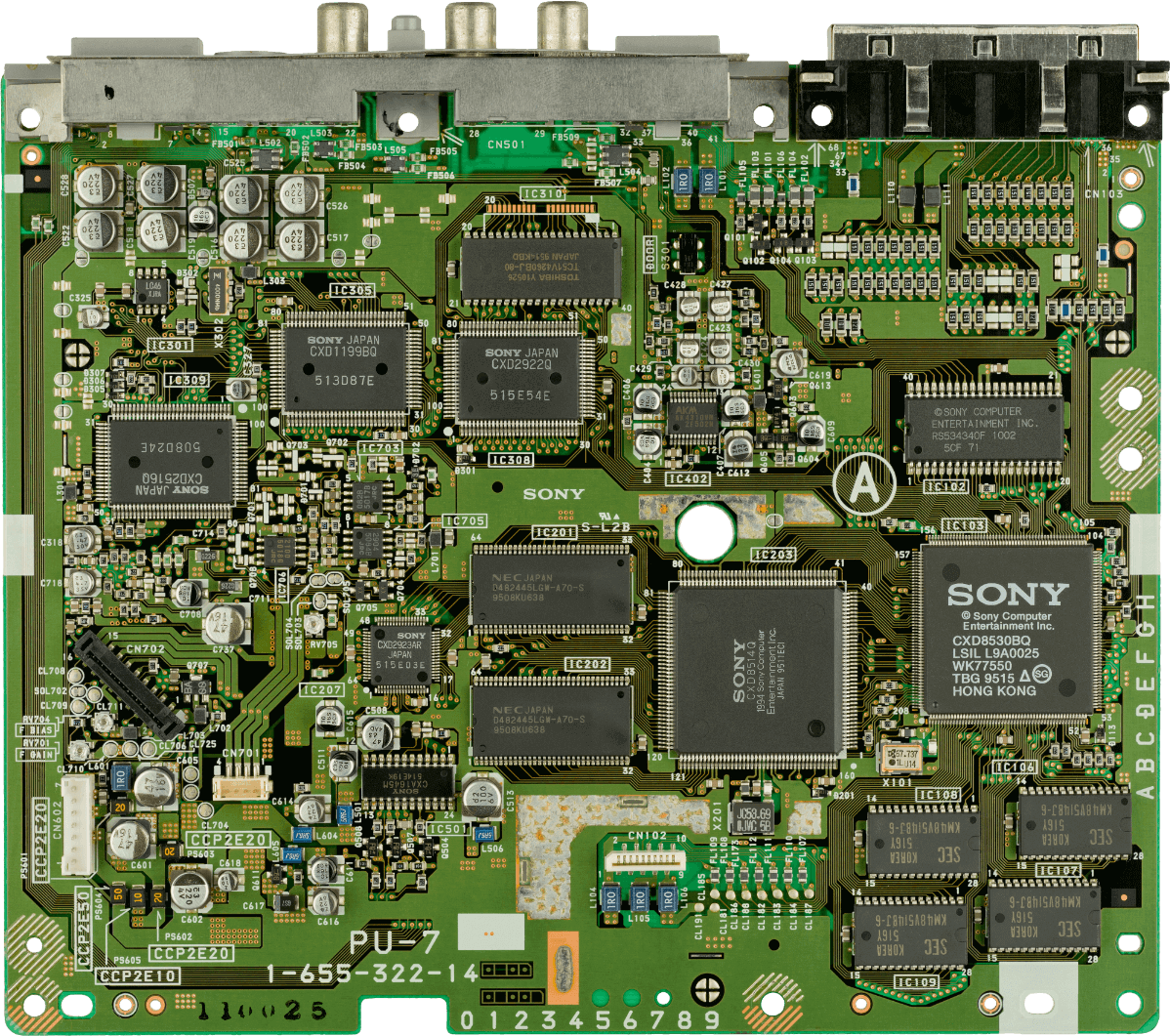
Showing model 'SCPH-1000'.
Remaining chips are fitted on the back.
Later models included SG-RAM instead of VRAM and removed most of the external I/O and video outs.
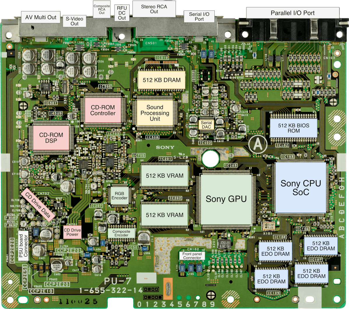
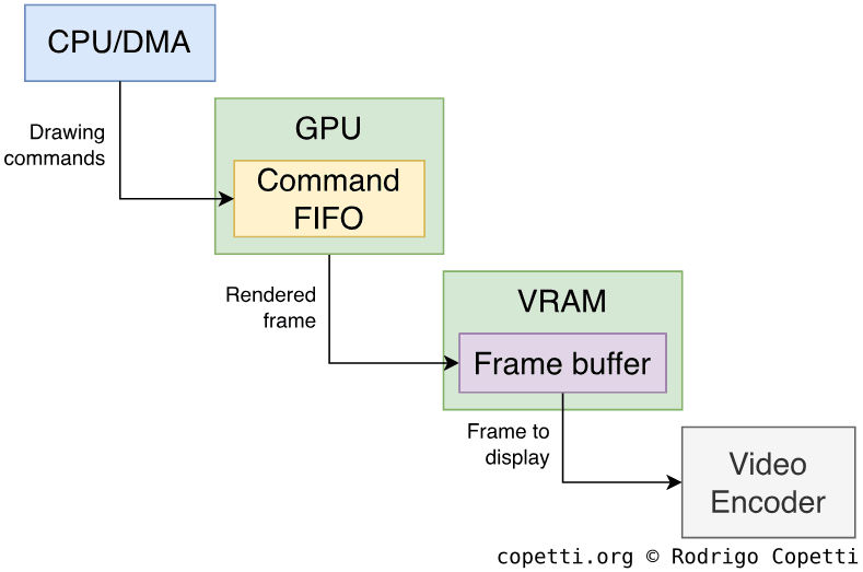
Diagram
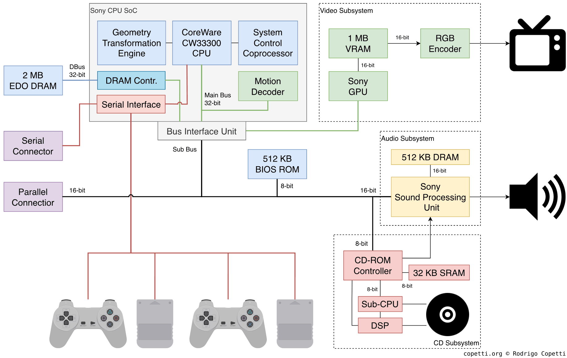
The Bus Interface Unit is also connected to special ports of the GPU and SPU.
A quick introduction
Sony knew that 3D hardware could get very messy to develop for. Thus, their debuting console will keep its design simple and practical… Although this may come at a cost!
CPU
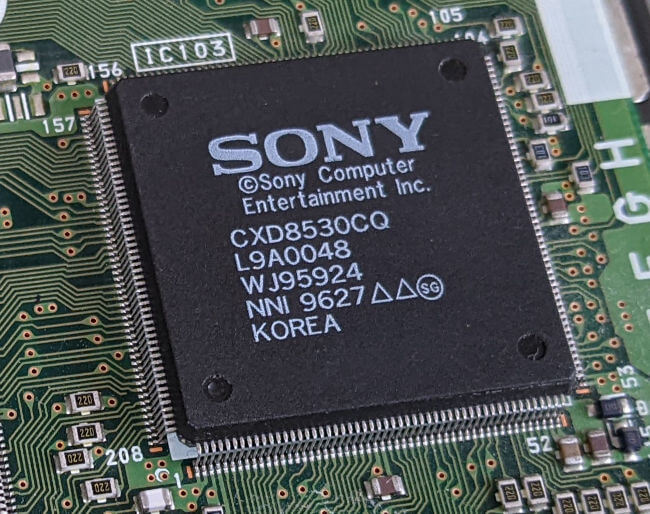
This section dissects the Sony CXD8530BQ, one of the two big chips this console houses. It’s what we would call a ‘System-on-Chip’ in today’s terms.
The origins
The main processor follows one of those ‘X designed by Y, based on Z, and second-sourced from W’ arrangements, which is a bit dense to summarise in just a few sentences. So, why don’t we start with some historical context?
A bit of history
The early nineties were marked by a turning point in the fortunes of many popular CPUs. The once-leading 8-bit processors, such as the Z80 and 6502, had already faded from the spotlight, and Motorola’s famous 68000, along with other 16-bit designs that enjoyed success in the late 80s, were now candidates for replacement. Even in the PC field at the time, Andrew S. Tanenbaum, in his celebrated debate with Linus Torvalds, predicted that Intel’s x86 architecture had only five more years left until its demise from the home market.
At first glance, it may look as though technological development had hit a wall. In reality, however, a new wave of relatively unknown CPUs was beginning to find its way into mainstream devices. Many of these designs originated in academia, and so intended to prove particular sets of design principles. Novel examples from that era include:
- MIPS: Adopted by Silicon Graphics Incorporated (targeting graphics workstations).
- PowerPC: Adopted by Apple (targeting desktop publishing).
- SPARC: Developed by Sun Microsystems (targeting servers and business workstations).
- ARM: Developed by Acorn, initially targeting the consumer market before expanding into PDAs, cell phones, and other embedded devices.
- … and many more ‘microcontroller’ chips that had yet to be finalised or adopted by a major industry - such as the Hitachi’s SH and NEC’s V810. To their surprise, these were subsequently selected for the Sega Saturn and the Nintendo Virtual Boy, respectively.
All of these processors had one thing in common: they adhered to the Reduced Instruction Set Computer (RISC) discipline, which radically shifted how such chips were designed and programmed. One rule of the RISC architecture dictated that a single instruction could not mix memory access with register operations. This allowed hardware designers to simplify the circuitry responsible for executing instructions… and then enhance it with parallelism techniques.
MIPS and Sony
MIPS Computer Systems originated from the eagerness of its founders (Stanford faculty) who were keen to turn their research into physical processors. This aligned well with the appetite of Silicon Valley venture capitalists in the 80s, who were anxious to invest in such innovations [2]. Their debuting CPU, the ‘MIPS R2000’, is considered the first commercial CPU to incorporate a RISC design, and it found a space in many UNIX workstations.
However, it wasn’t until 1987 that MIPS’ chips became a topic of conversation, all thanks to their adoption (and eventual acquisition) by Silicon Graphics Incorporated (SGI) to power its equipment. SGI was an influential force in the computer graphics market, especially with the development of hardware-accelerated vertex pipelines, a function originally carried out by software (within the CPU). Following the merger, SGI secured a leading position in both CPU and graphics sectors.
Prior to the development of the PlayStation, MIPS transitioned to a business model based on IP licensing, in which CPU designs were sold in the form of licenses, and licensees were then free to customise and manufacture the designs. Among their offerings was the R3000A CPU, found in their low-end catalogue. As such, the R3000A was not associated with the flagship line (unlike the R4000, which others would later choose), but it was an attractive investment in terms of cost.
Back to the main topic, Sony designed their audio and graphics chips in-house, but still needed the leading chip to drive those two. The selected CPU had to be powerful enough to showcase the impressive capabilities of Sony’s chips, while remaining affordable to keep the console at a competitive price.
LSI and the commission
At the same time, LSI Logic (a semiconductor manufacturer) was a MIPS licensee that provided a ‘build-your-own’ CPU programme for businesses. This service, known as CoreWare, enabled clients to assemble custom CPU packages by choosing from a series of building blocks [3]. Part of the CoreWare library included the ‘CW33300’ block, a CPU core derived from the LSI LR33300 - an off-the-shelf CPU chip that LSI also commercialised.
Now, where am I going with all this? It turns out both the LR33300 and CW33300 are a binary-compatible with the MIPS R3000A family. Their architectures differ slightly in some areas, but the programming interface (MIPS I ISA) remains the same.
In the end, Sony commissioned LSI to build their CPU package. They selected the CW33000, changed some bits, and integrated it with other blocks to form the chip you find on the PlayStation’s motherboard.
The offering
The resulting CPU core runs at 33.87 MHz and features:
- The MIPS I ISA: The first version of the MIPS instruction set architecture. Among many things, it uses 32-bit words and includes multiplication and division instructions.
- 32 general-purpose registers and 2 multiplication/division registers: These are 32-bit as well. One general-purpose register (
R0) is hardwired to zero, a common trait in RISC designs. - 32-bit data bus: In the PS1, this bus branches into two:
- Main Bus (32-bit): Connects the MDEC and GPU.
- Sub Bus (16/8-bit): Connects the remaining components and I/O. This bus is bridged by the Bus Interface Unit, which also enables access to special ports of the GPU and SPU.
- 32-bit address bus: Enables access of up to 4 GB of physical memory. In other words, RAM, memory-mapped I/O, etc.
- 5-stage pipeline: Allows up to five instructions to be processed simultaneously (see a previous article for a detailed explanation).
- 4 KB of instruction cache: This can be ‘isolated’ as well, allowing the program to manipulate the instruction cache directly.
- Oddly, there is no data cache. The 1 KB of memory normally reserved for it is mapped to a fixed address [4]. This area is called Scratchpad and it’s used as ‘fast SRAM’.
To do something meaningful, Sony provided 2 MB of RAM for general-purpose use. Curiously enough, they fitted Extended Data Out (EDO) chips on the motherboard. These are slightly more efficient than typical DRAM, obtaining lower latency.
Taking over the CPU
At certain points, any subsystem (graphics, audio or the CD drive) will require large chunks of data at a fast rate. However, the CPU is not always capable of keeping up with the demand.
For this reason, the CD-ROM controller, MDEC, GPU, SPU and the parallel port are granted access to a dedicated DMA controller whenever they require it. Direct Memory Access (DMA) takes control of the main bus to perform data transfers independently. This results in significantly higher throughput than routing the transfer through the CPU, although the latter is still required to set up the DMA operation.
It’s also worth noting that once the DMA kicks in, the CPU is unable to access the main bus. This means the CPU will be idling unless it’s got something in Scratchpad to keep itself busy!
Complementing the core
Like other MIPS R3000-based CPUs, the CW33000 supports configurations with up to four coprocessors. Sony customised it with three:
System Control Coprocessor
Identified as ‘CP0’, the System Control Coprocessor is a common block found in MIPS CPUs. In R3000-based systems, like this one, the CP0 governs how the cache is implemented. Thus, enabling direct access to the data cache (in the form of ‘Scratchpad’) and instruction cache (through ‘cache isolation’). The control coprocessor also handles interrupts, exceptions and breakpoints - the latter is useful during debugging.
Wait, shouldn’t coprocessors only expand CPU functions? Why is CP0 tightly coupled with the CPU?
Indeed, R3000 cores depend on the system control coprocessor to make use of many components. Whether or not this should be ‘legal’ comes down to the interpretation of the word ‘coprocessor’. According to MIPS, a coprocessor is not strictly an optional part of the CPU - it may also command the CPU’s surroundings (e.g. cache, interrupts). Hence, a coprocessor can be an integral part of the system. This is something to bear in mind when discussing MIPS-related systems.
Later R4000-based systems incorporated a Memory Management Unit (MMU) and a Translation Lookaside Buffer (TLB) into this block, thereby increasing its capabilities and taking up new roles.
Geometry Transformation Engine
The ‘CP2’, or Geometry Transformation Engine (GTE), is a specialised math processor that accelerates vector and matrix calculations.
While only operating fixed-point types, it still provides useful operations for 3D graphics, such as:
- Matrix or vector multiplication, addition, and vector square.
- Perspective transformation (used for 3D projections).
- Outer product of two or three vectors (the latter is used for clipping).
- Many interpolation functions that use different parameters.
- Depth cueing and colour value derived from a light source (used for lighting and colour operations).
- Z/depth averaging. I suspect this is used for the ‘ordering table’ (I explain more details in the ‘Graphics’ section).
You don’t need to memorise all of this to follow the rest of the article! Just keep in mind that the GTE takes care of the initial stages of the graphics pipeline, including 3D projection, lighting, and clipping. This will help to generate the required data to send to the GPU for rendering.
Motion Decoder
The Motion Decoder, also called ‘MDEC’ or ‘Macroblock Decoder’, is another processor living next to the CPU. This time, it decompresses ‘macroblocks’ into a format the GPU can understand. A macroblock is a data structure containing an image encoded similarly to JPEG.
The MDEC decompresses bitmaps consisting of 8x8 pixels at 24 bpp (bits per pixel). Overall, the MDEC can compute 9,000 macroblocks per second [5], enabling to stream a 320x240 px Full-Motion Video (FMV) at 30 frames per second.
DMA is used to transfer compressed data through the CD-ROM, RAM, and MDEC. The same path is used in reverse, though the destination in this case is VRAM.
While this component resides within the SoC and shares the same data bus, it is not a MIPS coprocessor; the CPU and DMA access it via the memory map, rather than intercepting instructions.
For more info about the MDEC unit, I suggest consulting Sabin’s [6] and Czekański’s [7] resources.
Missing units?
So far, we’ve seen a ‘CP0’ and a ‘CP2’, but where’s the ‘CP1’? Well, that’s actually reserved for a Floating-Point Unit (FPU) - and I’m afraid Sony didn’t provide one. This doesn’t mean the CPU is incapable of performing arithmetic with decimal numbers; it simply won’t be fast enough (when using software routines) or particularly accurate (when relying on fixed-point arithmetic).
Game logic (involving physics, collision detection, and similar) can still get by using fixed-point arithmetic. Fixed-point encoding represents decimal numbers with an immutable number of decimal places. This leads to a loss in precision during certain operations, but remember: this is a video game console, not a professional flight simulator. Hence, the trade-off between precision and performance can be considered reasonable.
By the way, if you’d like a quick refresher on concepts like ‘fixed-point’, ‘floating-point’, ‘decimal’, and ‘integer’, I recommend taking a look at Gabriel Ivancescu’s post [8].
Delay galore
As we’ve seen before, the CW33300 is a pipelined processor - meaning it queues multiple instructions and executes them in parallel at different stages. This hugely improves instruction throughput, but without proper control, it can lead to pipeline hazards, resulting in computational errors.
The MIPS I architecture is particularly susceptible to [9]:
- Control hazards: Instructions may get executed when they shouldn’t.
- Data hazards: Instructions may operate with outdated data before it’s been updated.
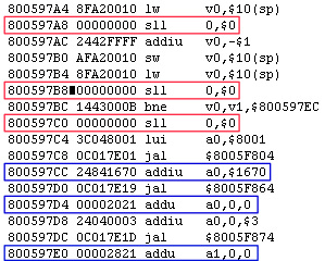
LW (load word from memory), JAL (jump and link) and BNE (branch on not equal) are each followed by a delay slot to prevent hazards. Instructions marked in red (found before address 800597C4) are fillers (useless instructions), while the rest marked in blue perform meaningful computations.Consequently, MIPS I CPUs exhibit the following behaviour:
- Any instruction following a ‘branch’ or ‘jump’ opcode is executed unconditionally: Thus, developers have to manually fill the pipeline with modest instructions (such as
calculate 0 plus 0) after the branch or jump to mitigate the hazard. These fillers are called branch delay slots.- Modern CPUs converted this phenomenon into an advantage: Branch prediction. By adding circuitry to detect the hazard, the CPU can discard speculative computations if the branch or jump condition isn’t met. But if it holds true, then the CPU saves time.
- ‘Load’ instructions don’t stall the pipeline until the retrieved data becomes available: The second stage of the pipeline (called
RDor ‘Read and Decode’) gathers the operands that will be used during the third stage (ALU) [10]. The fourth stage (MEM, from ‘access MEMory’) looks for data in memory (e.g. main RAM or the CD reader). Now, here’s the problem: by the time aloadinstruction gathers the data from outside, the next instruction already fetched the operands. Therefore, when an instruction depends on the data from a precedingload, a filler must be inserted to ensure the correct operands are fetched on time.
As illustrated in the example, some delay slots are filled with meaningful instructions, which perform computations that are not affected by the hazard. Hence, delay slots do not always equate to wasted cycles.
A core philosophy
Having explained this, you may be wondering why a processor exhibiting such flaws would ever be commercialised. Well, one tenet of the RISC philosophy is that the burden of CPU programming is shifted from the developer to the compiler. MIPS, in particular, prioritised the production of high-quality compilers (including assemblers) to accompany their new CPUs [11]. Hence, the company envisioned that developers would use a higher-level language (like C) while the toolchain automatically dealt with hazards, either by reordering instructions to fill in slots, or by adding useless fillers as a last measure.
In fact, exposing the CPU pipeline to developers was an core design strategy at MIPS, evidenced by its very initials standing for ‘Microprocessor without Interlocked Pipelined Stages’.
So, all in all, while I don’t find it pleasant to see a program filling the CPU with bubbles, I think MIPS tackled this challenge in a very ingenious way. That said, it wasn’t without its disadvantages, however. As later years revealed, exposing the pipeline made backwards compatibility very tricky, especially as future CPUs debuted revolutionary microarchitectures.
Graphics
To recap, a large part of the graphics pipeline is carried out by the GTE. This includes perspective transformation (which projects the 3D space onto a 2D plane using the camera’s perspective) and lighting. The processed data is then sent to Sony’s proprietary Graphics Processor Unit (GPU) for rendering.
Organising the content
The system features 1 MB of Video RAM (VRAM) that will be used to store the frame buffer, textures, and other resources the GPU will require to render the scene. The CPU can populate this area using DMA.
The type of chip fitted (VRAM) is dual-ported, like the Virtual Boy’s. VRAM uses two 16-bit buses, which enables concurrent access by the CPU, DMA, GPU and the video encoder.
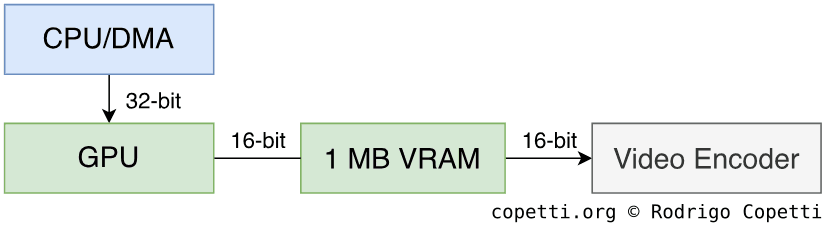
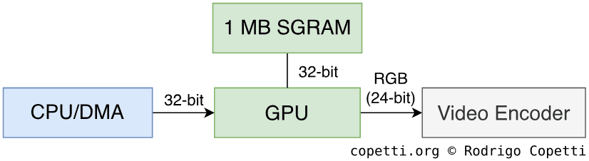
Though in later revisions of this console, Sony switched to Synchronous Graphics RAM (SGRAM) chips (the single-ported alternative, using an individual 32-bit data bus). Boo!… Well, to be fair, each one comes with its pros and cons.
One thing for sure is that, due to timing differences, later games (such as Jet Moto 3) display glitched graphics when run on VRAM-based systems. If you want to know the details, Martin Korth’s ‘Nocash PSX Specifications’ document the various timings and such [12].
Drawing the scene
If you’ve been reading the Sega Saturn article, let me tell you that the design of this GPU is a lot simpler! For starters, the GPU is made of a single chip.
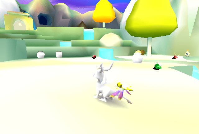
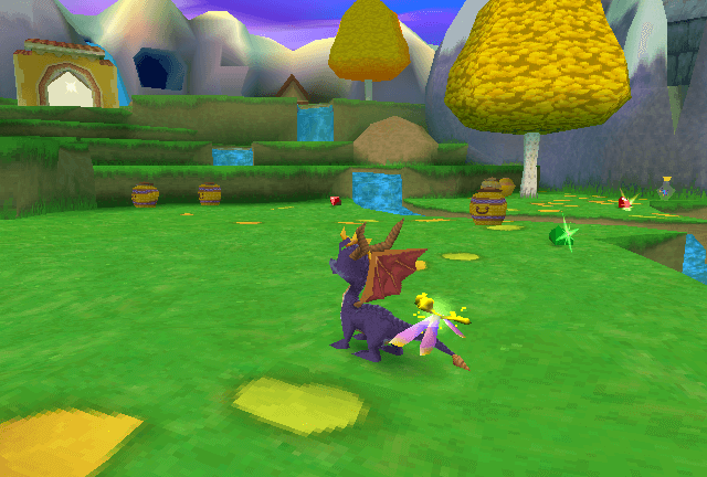
Now, to show how a scene is drawn, I will mainly use Insomniac’s Spyro: Year of the Dragon as an example.
Commands
To start with, the CPU sends geometry data (vertices) to the GPU by filling its internal 64-byte FIFO buffer with commands (up to three). These commands may request to GPU to render something, change a setting or manipulate VRAM.
Essentially, a render command states how and where to draw a primitive. The GPU can draw lines, rectangles and triangles individually - the latter being the fundamental ingredient for constructing rich 3D models.
Once the geometry is received, clipping is applied to skip operations on unseen polygons (residing outside the camera’s viewport).
The position of each primitive is defined using an X/Y coordinate system that maps directly to the frame buffer. The PS1’s GPU employs an integer coordinate model, in which each coordinate corresponds to the centre point of a pixel (known as sampling point). In other words, there are no fractional coordinates.
Visibility approach
Just like the competition, the PS1 doesn’t include any hardware feature that tackles the visibility problem. Nonetheless, the GPU handles sorted polygons by providing an ordering table: a dedicated structure in which each entry is indexed by a depth value (also called ‘Z-value’) and contains the address where the corresponding GPU command resides [14].
The CPU must manually sort the polygons first, and then place references in the appropriate entries of the table. Finally, the CPU orders the DMA to send the table to the GPU. This process enables the GPU to render the geometry in the correct order.
Multiple DMA functions are also provided to assist both the CPU and GPU with the creation and traversal of this table.
Rasterisation
Once the commands are decoded by the GPU, it’s time to convert the received geometry (vertices) into pixels. This enables the system to apply texture mapping and effects, ultimately displaying the result on a two-dimensional panel (such as your TV or monitor). To do this, the GPU allocates a pixel matrix as its working area, this is called a frame buffer. Compared to the more complex Sega Saturn, the GPU requires only a single frame buffer.
The rasteriser is the unit in charge of converting vectors into lines, triangles, or rectangles - and finally into pixels. Now, the process differs drastically depending on the requested primitive [15]:
- Triangles are the most complex (and versatile) type, which can be textured and shaded.
- Lines are quicker to draw but naturally unsuitable for textured surfaces. Shading is still supported.
- Rectangles are also faster but can only fit a sprite of up to 256 x 256 pixels; larger rectangles will only duplicate the sprite’s graphic. Even so, they offer no affine transformation (aside from X/Y flipping), nor shading or effects. I suspect rectangles were only implemented to assist the development of 2D games.
In the case of the triangle, being the only textured polygon, the rasteriser will:
- Grab each three-point vertex and calculate the edges. This forms a triangle.
- Analyse the triangle’s area to determine which pixels of the frame buffer they occupy. Only the portion of the polygon covering the sampling points get turned into pixels.
The generated pixels are not written into the frame buffer right away. Instead, they are passed to the next stages of the pipeline for further processing. I cover this in the subsequent paragraphs.
Shaders
In order to apply lighting effects to triangles or lines, the GPU offers two algorithms:
- Flat shading: Each primitive has a constant light level.
- Gouraud shading: Each vertex embeds its own light level. Then, the brightness is automatically interpolated between points.
- As you can imagine, this type offers more realistic results than flat shading.
The rationale behind providing this choice comes down to performance: flat shading fills ~2.5 times more polygons per second than Gouraud shading. Thus, it’s important to optimise which polygons truly benefit from more realistic lighting than others.
Textures
Triangle surfaces may also be blended with textures (2D bitmaps) to produce the final result.
The GPU performs inverse texture mapping, where it traverses each rasterised pixel and looks for its corresponding pixel in the texture map (called texel). Texels are calculated by linearly interpolating the texture map (found in VRAM) to match the shape of the polygon. The interpolation routine is called Affine Texture Mapping, which operates solely on 2D coordinates (X and Y values), discarding the third coordinate (Z or ‘depth’) that would otherwise account for perspective.
Because texture maps rarely match the exact dimensions of rasterised polygons, aliasing (incorrect rendering results) tend to appear. This manifests as unwanted distortions, such as missing or oversized texels. To remedy this, sophisticated GPUs employ texture filtering to smooth out (interpolate) abrupt colour changes. Now, the PS1’s GPU does not implement any filter, so it resorts to an algorithm known as nearest neighbour to correct scales without smoothing out the results. This is very fast and cheap, but it also explains why textured models may look ‘blocky’.
The GPU also supports the following effects, available for use on triangles:
- Semi-transparency: Simulates light passing through overlapping textures.
- Dithering: Softens sudden changes in colour while adhering to the same colour palette.
It’s worth noting that the PS1 happened to excel at these effects!
Remaining steps
Once finished, the GPU writes the pixels to the frame buffer area in VRAM, which is in turn picked up by the video encoder and broadcasted to the screen.
Designs
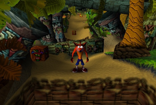
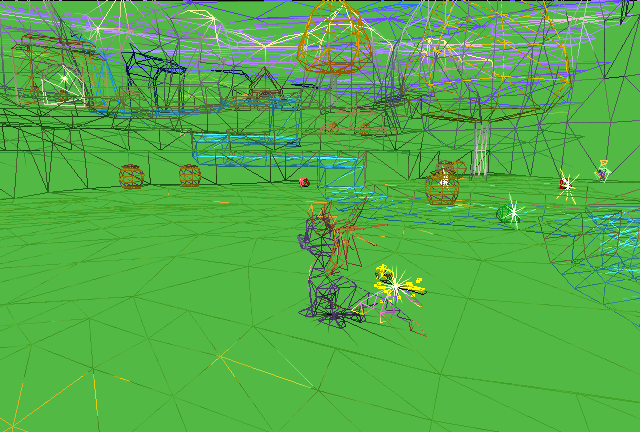
Let’s take a break now from all this theory. Here are some examples of game characters designed specifically for the 3D era. Notice the use of triangles and nearest-neighbour textures. I encourage you to compare them with the models featured in the other articles.


 Interactive model available in the modern edition
413 triangles.


 Interactive model available in the modern edition
732 triangles.
Playing with VRAM
Given the available amount of VRAM (a whole megabyte), one could allocate a massive frame buffer of 1024×512 pixels with 16-bit colours, or a realistic one of 960×512 pixels with 24-bit colours - allowing to draw some of the finest frames ever seen in gaming… This sounds pretty impressive, right? Well, it does raise a few issues, for instance:
- These dimensions would need to be rescaled to comply with standardised formats (e.g. 480i NTSC or 576i PAL), so the video encoder can broadcast them on consumer TVs.
- How is the GPU supposed to render anything decent if there isn’t any space left for other assets (e.g. textures and colour tables)?
- The PS1’s GPU can only render frame buffers of up to 640×480 pixels and 16-bit colours.
All right, let’s use a 640x480 buffer with 16-bit colour instead, which leaves 424 KB of VRAM for materials. So far, so good? Again, such resolution may look fine on CRT monitors, but it’s not particularly noticeable on those 90s TVs everyone had in their homes. Then, is there any way to optimise the frame buffer? Introducing adjustable frame-buffers.
In essence, rather than wasting valuable VRAM on ‘unappreciated’ resolutions, this console’s GPU allows to decrease the dimensions of the frame buffer to effectively increment the space available for other resources. In a demonstration from ‘Gears Episode 2’ [16], Halkun shows a setup that divides the 640x480 frame buffer into two 320x480 ones, employing a technique called page flipping to render multiple scenes at the same time.
Page flipping involves alternating the location of the frame for display between two buffers whenever required, allowing the game to render one scene while displaying another. Thus, hiding any flickering effect and improving loading times (something that the player will certainly appreciate!).
Overall, Halkun’s layout consumes only 600 KB of VRAM. The remaining 424 KB can be used to store colour lookup tables and textures which, paired with 2 KB of texture cache available, result in a very convenient and efficient setup.
Finally, it is also worth mentioning that VRAM can be mapped using multiple colour depths simultaneously, meaning that programmers can allocate a 16 bpp frame buffer next to 24 bpp bitmaps (commonly used by FMV frames, for instance). This is another avenue for further optimisation of space.
Secrets and Limitations
Whereas the PS1 had a straightforward and suitable architecture, problems still arose. Surprisingly, certain issues were tackled through rather clever workarounds.
Distorted models/textures
The routines used for handling geometry and applying textures are known to carry some inaccuracies.
Firstly, the rasteriser only handles pixel units: While vertex coordinates are expressed as integers, the calculated triangle edges may occupy only a fraction of a pixel. However, the rasteriser will draw the pixel only if the triangle’s area covers the pixel’s sampling point, and it does not keep track of the fraction occupied [17]. This brings up some problems:
- The outer edges of models will make sudden jumps when moved slightly.
- Triangles within a mesh (which share the same vertices and edges) will often ‘compete’ to draw over the same pixels. Taking into account the ordering table, the GPU renders following a ‘last-come, first-served’ basis, which will cause triangle intersections to flicker or overlap when moved slightly.
This is commonly tackled by implementing sub-pixel resolution, which allows the rasteriser to keep track of the fractions of pixels occupied by each triangle area [18]. As a result, anti-aliasing methods can then be applied to soften jagged edges or abrupt changes in colour.
Moving on, the ordering table puts the burden on the developer/program to show the geometry in the right order. In some cases, the underlying calculations rely on excessive approximations to gain performance. This may result in flickering or occluded surfaces that ought to have been displayed.
Furthermore, setting a low-resolution frame buffer can amplify all these aliasing issues.
Finally, as you know, affine transformations lack any sense of depth. This may confuse the user’s perception, especially when the camera is positioned close to the model and perpendicular to the viewer’s line of sight [19]. The anomaly is known as texture warping. Hence, some games resorted to tessellation (splitting large polygons into smaller ones) to reduce distortion, while others opted to swap textures with solid colours. In general, a GPU ultimately tackles this issue by implementing perspective correction, which interpolates textures using the depth value.
Contradicting claims
If you check other technical channels or forums, you’ll find alternative explanations for the PS1’s wobbling, warping, and distortion effects. While some may align with my previous explanations, others argue differently. Therefore, I’d like to offer my perspective on why the following statements are inaccurate:
Models and textures wobble due to lack of an FPU
An FPU does not dictate whether a system can operate fractional numbers. The PS1, like any other computer without a hardware FPU, can still perform fixed-point arithmetic. Furthermore, floating-point numbers can also be computed (just slower) through software. In essence, FPUs are accelerators, do not confuse them with the concept of decimal numbers or with an ALU (the critical portion of a CPU responsible for arithmetic operations).
Models and textures wobble due to the GPU’s integer coordinate system
Employing integer coordinates is a common approach to make calculations less expensive in the GPU. What turns this into a visible problem is the lack of sub-pixel resolution. This is because anti-aliasing can be applied to smooth out sudden changes of colours - provided the rasteriser tracked the fraction of the pixel occupied by the triangle.
Textures warp due to lack of mipmapping
GPUs that implement inverse texture mapping, such as this one, are subject to a measurement error known as ‘undersampling’ (one pixel is mapped to multiple texels). This produces aliasing (wrong results). The behaviour is noticeable when rendering geometry located far from the camera. To remedy this, modern texture mappers apply ‘trilinear filtering’, which softens texels using the same texture stored at different scales (mipmaps) and does some interpolation in-between. To sum up, mipmapping is a method for reducing aliasing. It is affine texture mapping (with its lack of perspective correction) that interpolates textures on three-point surfaces without taking into account the depth. Hence, the ‘warping’ effect.
Models and textures flicker due to lack of Z-buffering
A GPU equipped with a Z-buffer solves the visible surface determination problem at the hardware level. In contrast, the PS1 relies on an ordering table, meaning developers are in charge of determining what geometry is in front of other. In short, flickering triangles are caused by the sorting routines (software).
Pre-rendered graphics
Let’s highlight a positive feature now for a change…
When a game strived for a more realistic scenery than the GPU could provide in real time, one available option was to stack two triangles and use the Motion Decoder to stream pre-rendered cinematics onto them. FMV sequences required lots of storage space, but luckily, the CD-ROM was well-prepared for this.
Some titles relied on this technique to compose backgrounds and, honestly, it looked quite convincing on a CRT television. Of course, modern emulators with upscaling capabilities will tell on very quickly.
Video out
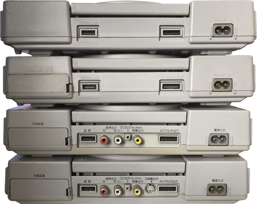
The first revision of this console carries a surprisingly wide range of video signals, accessible via the following ports:
- RFU DC: Designed to connect an RF modulator.
- RCA: Outputs composite video and stereo audio.
- S-Video: Provides a combined Luma + Sync, and a separate Chroma signal.
- AV Multi Out: Offers all the aforementioned signals, excluding RFU. It additionally carries RGB and a 5+ Volts line.
In subsequent revisions, most of these ports were phased out, leaving only the ‘AV Multi Out’ on late models.
Audio
Sony’s signature Sound Processing Unit (SPU) takes care of this. This chip supports the enormous amount of 24 channels of 16-bit ADPCM samples (a more efficient version of the well-known PCM sampling) with a sampling rate of 44.1 kHz (Audio CD quality).
This chip also provides the following capabilities:
- Pitch modulation: As the name suggests, games can automatically alter the pitch of their samples instead of storing additional ones. This is useful for music sequencing.
- Frequency modulation: Channels can be assigned to modify the frequency of others. This is comparable to FM synthesis.
- ADSR Envelope: These are a set of parameters available for amplitude modulation.
- Looping: Instructs the system to play a piece of audio repeatedly.
- Digital reverb: Simulates the sample being played in a specific acoustic environment to enhance immersion.
512 KB of DRAM (called ‘Sound RAM’) is provided as an audio buffer. This memory is accessible by the CPU (via DMA) and the CD controller. Nevertheless, games have access to only 508 KB to store samples, while the rest is reserved by the SPU to process Audio CD music. This amount is further reduced when reverb is enabled.
The CD controller can also send samples directly to the audio mixer without passing through the audio buffer or requiring CPU intervention. Samples can also be compressed using ‘XA’ encoding, which the SPU can decode in real time.
The streaming era
Similarly to the Saturn, games are no longer dependent on music sequencing or predefined waveforms, and thanks to the extensive storage available on the CD-ROM medium, developers can store fully produced samples and just stream them directly to the audio chip.
I/O
Two I/O ports - Serial and Parallel - were originally available for add-ons. However, these were removed in later revisions of the console due to low adoption and concerns that they could be exploited to bypass the copy protection system.
CD subsystem
The block responsible for controlling the CD drive is an interesting area, you can imagine it as a separate computer living inside the PlayStation.
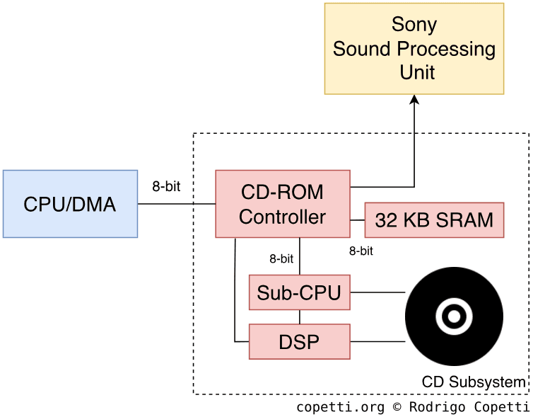
This subsystem comprises:
- A DSP: Controls the motor and laser, and processes the RF signal coming from the laser.
- A Sub-CPU: A CPU package made of a Motorola 68HC05 microcontroller, 512 B of RAM, and 16 KB of ROM [21]. In a nutshell, the Sub-CPU runs a local program stored in ROM and controls the DSP. The Sub-CPU program implements copy-protection measures and they are enforced whether the main CPU ‘likes it or not’.
- A CD Controller: Serves as the middle-man between the CD subsystem and the rest of the console, receiving commands from main CPU (in a FIFO manner) and triggering interrupts after specific events. As a controller, the chip talks to the Sub-CPU and receives CD data from the DSP.
- Furthermore, the controller bundles a DMA unit that is connected to the SPU, which allows it to stream audio directly.
- 32 KB of SRAM connected to the controller: This is presumably used as a buffer for data read from the disc.
The subsystem somewhat resembles the typical CD drive everyone had at their home, albeit with particular tweaks Sony implemented in the Sub-CPU program to perform anti-piracy checks.
Front ports
The console features four front-facing sockets: two for game controllers and two for Memory Cards (used to store game saves). All four slots are electrically identical [22], so the address of each one is hardcoded. Additionally, Sony altered the physical shape of the ports to avoid accidents.
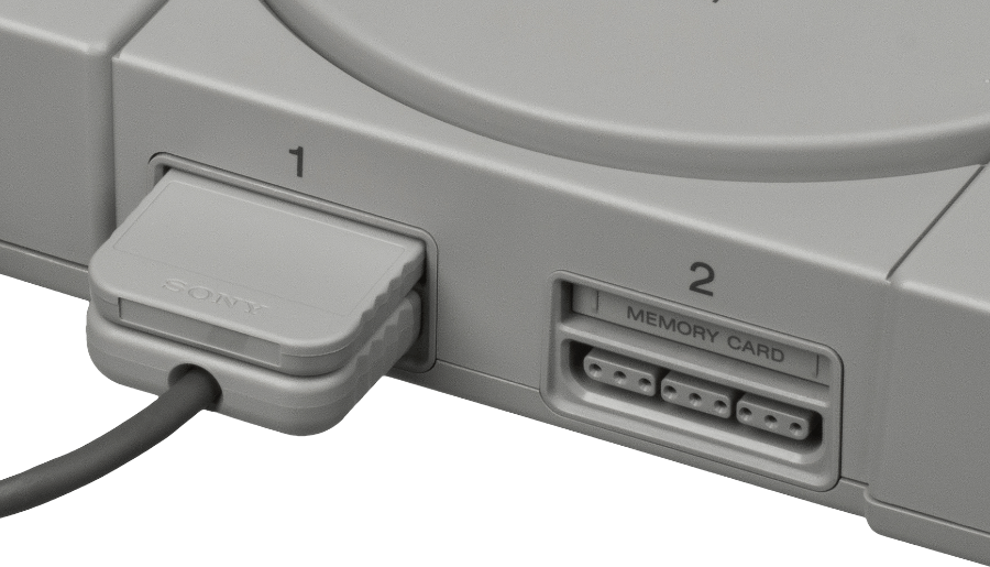
Communication with these devices is accomplished through a serial interface. Commands sent by the console are delivered to one of the two groups (either ‘mem. card 0’ and ‘controller 0’, or ‘mem. card 1’ and ‘controller 1’). The two accessories answer with their unique identifiers, allowing the console to focus on a particular type of device (memory card or controller) from that point onward.
Operating System
The system includes a 512 KB ROM that stores a ‘BIOS’. This program performs many services, including taking care of the startup process, displaying the user shell, and exposing a collection of I/O routines [24].
BIOS/Kernel
The BIOS is a critical dependency for games. Not only this program bootstraps them from the CD drive, it also acts as an intermediary to interact with the console’s hardware. This methodology resembles IBM’s implementation of their IBM PC BIOS, which encouraged developers to use a standard interrupt table (containing I/O routines) instead of relying on platform-dependent I/O ports.
Having said that, the PS1 BIOS exposes routines such as:
- Commands for the CD-ROM drive.
- Filesystem operations for the CD-ROM and Memory Card.
- Multithreading.
- Standard C functions (e.g. string manipulation and memory operations).
Since access to the BIOS ROM is very slow (as it’s connected via an 8-bit data bus), the APIs are packaged in the form of a Kernel and copied to main RAM during boot. Thus, 64 KB of main RAM are reserved for the Kernel, also referred to as PlayStation OS.
Boot process
The CPU’s reset vector is located at 0xBFC00000, which points to the BIOS ROM.

Similar to the Saturn’s boot process, once powered on, the PS1 will:
- Look for the BIOS ROM and execute routines to initialise the hardware.
- Load PlayStation OS.
- Display the splash screen.
- If there is a CD inserted, the CD-ROM controller will check if it’s genuine:
- It is: The controller will allow to read its contents. In turn, the CPU will look for a file named
SYSTEM.CNF(which specifies the location of the executable and some metadata), and continue execution from there. - It’s not → The CPU will display an error message.
- It is: The controller will allow to read its contents. In turn, the CPU will look for a file named
- With no CD inserted, the CPU will display the shell.
- The user is now in control.
The shell is a simple graphical interface that allows the user to copy or delete saves from the memory card; or play an audio CD.
Games
Just like the Sega Saturn and other consoles that made the switch to the CD format, PS1 games benefit from a new set of facilities: large storage (620 MB, in the case of the PS1), rich audio quality and a ‘not-so-slow’ read speed thanks to its 2x drive.
If you are curious about how Compact Discs (CDs) work, I’ve written a brief explanation in the Sega Saturn article.
Be as it may, PS1 revisions released up to 1997 (three years after the console’s debut) were notorious for bundling a faulty CD drive laser [25], which resulted in frequent FMV and audio CD ‘skips’. Later models fixed the laser unit and improved the housing, mitigating the problem.
Development ecosystem
Sony distributed an SDK to game studios comprising a C compiler and libraries. The latter were linked to BIOS routines for hardware access. As a side note, this level of abstraction later helped emulate the PS1 across a wide range of platforms - both official and unofficial.
Alongside the SDK, Sony also provided specialised hardware such as the DTL-H2000: a dual-slot ISA card containing the internals and I/O of the PS1 [26], plus extra circuitry for debugging purposes. The board could access to the host’s hard drive and execute PS1 software without restrictions. The accompanying software required a PC with Windows 3.1 or 95 installed.
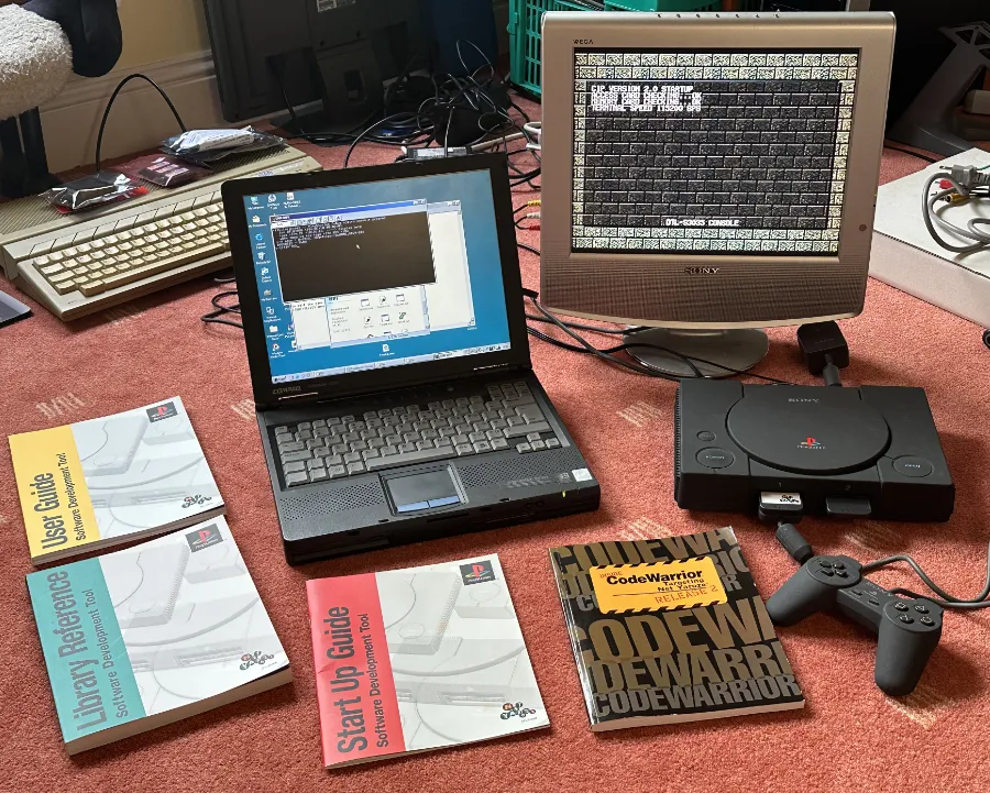
Two years after the release of the PS1, Sony shipped a developer kit for hobbyists called Net Yaroze. In addition to the toolkit and manuals, it included a black-coloured PS1 console. The latter bundled a modified copy-protection system, allowing only Net Yaroze software to boot. The software was transferred from an external computer via the serial port and loaded into the PS1’s main memory. The most significant limitation, when compared to studio-level devkits, was that the Net Yaroze did not provide access to the CD drive. This forced homebrew software to completely reside in main RAM (adding overhead).
Anti-piracy / Region Lock
As you may know, to fetch data from a CD, a laser beam is used to detect the pits and lands embedded in the disc’s track.
Now, conventional discs are not perfectly flat and often contain tiny fluctuations in their tracks. These defects are completely unnoticeable during reading, as the laser can automatically calibrate itself as it reads.
This is what Sony based their copy protection on: the Sub-CPU only reads discs whose particular track - the Table of Contents (TOC) - is engraved using a defined frequency, informally known as Wobble Groove. This frequency is introduced during the mastering process and cannot be replicated by conventional CD burners. The TOC resides in the inner section of the CD (called ‘Lead-In’ area) and instructs the laser on how to navigate throughout the disc [28]. Moreover, it is repeated multiple times as a fault-tolerance mechanism.
Within the game’s table of contents, one of the following character strings is embedded:
- SCEA, meaning ‘Sony Computer Entertainment of America’.
- SCEE, meaning ‘Sony Computer Entertainment of Europe’.
- SCEI, meaning ‘Sony Computer Entertainment of Japan’.
As you can guess, this technique was applied for region-locking as well.
Defeat
Conversely, this check is only executed once at the start, meaning that manually swapping the disc immediately after verification can bypass this protection - albeit with the risk of damaging the drive.
Later on, some games took matters into their own hands and often reinitialised the drive during gameplay, forcing the check to be performed again. This was done to prevent users from performing the ‘swap trick’.
Alternatively, tiny commercial boards programmed to mock the Wobble Groove signal could be soldered into the console. Known as Modchips, these components - while legally contentious - became incredibly popular.
Retaliation
The widespread availability of modchips, CD burners, and emulators were viewed as a significant threat by publishers. In response, later games included their own protection measures (mostly checksums) to deter any type of unauthorised use or modification.
One such method I was told about involved deliberately reinitialising the CD drive and then making it read specific sectors that would fail the Wobble Groove check. If this managed to unlock the drive regardless, the game (still residing in RAM) would happily unveil its anti-piracy material. Notably, this approach could also affect modified consoles using genuine discs.
Later on, Sony provided a library called Libcrypt, which fortified copy protection with the use of two approaches [29]:
- From the hardware side, checksums of specific sectors were stored in sub-channels of the disc.
- CD-ROM sub-channels traditionally store metadata, mostly to guide the drive. These are not user-accessible and conventional readers rarely allow to manually write over them.
- From the software side, a set of routines were embedded at different points of the game. These fetch the checksum values and mix them with others to perform verifications, in an attempt to counteract both emulators and pirated discs.


