Supporting imagery
Model
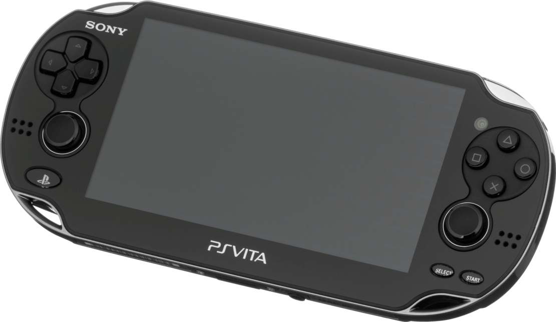
Released on 17/12/2011 in Japan, 12/02/2012 in America and 22/02/2012 in Europe.
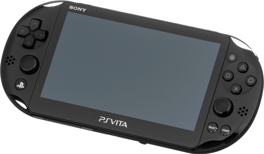
Released on 10/10/2013 in Japan, 07/02/2014 in Europe and 06/05/2014 in America.
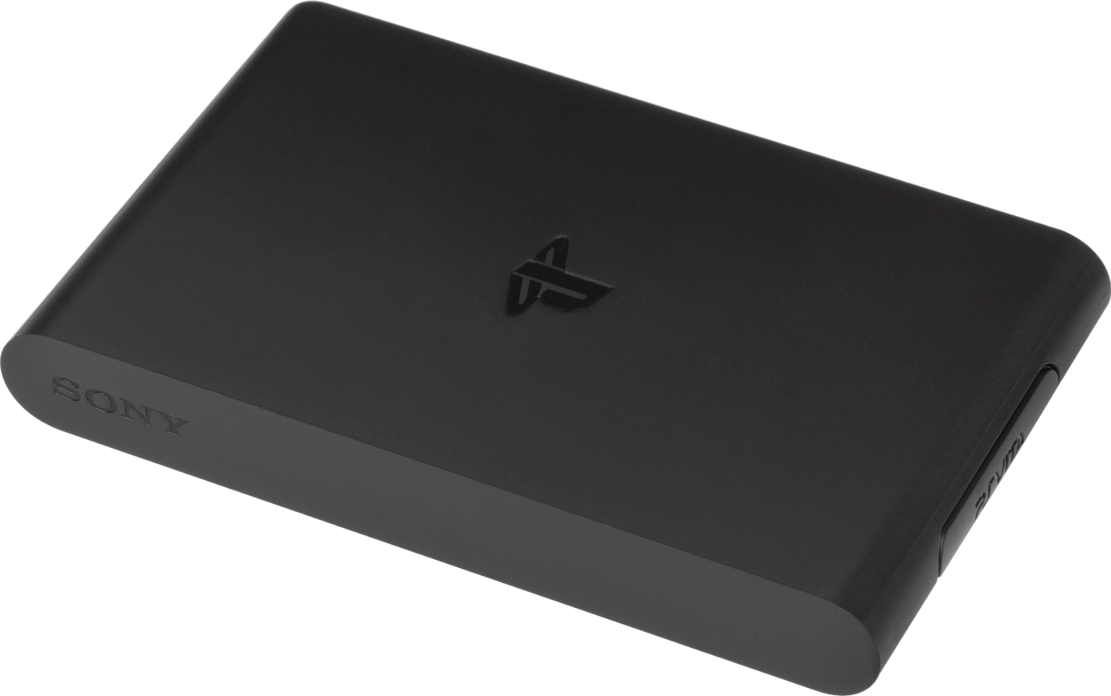
Released on 14/11/2013 in Japan, 14/10/2014 in America and 14/11/2014 in Europe.
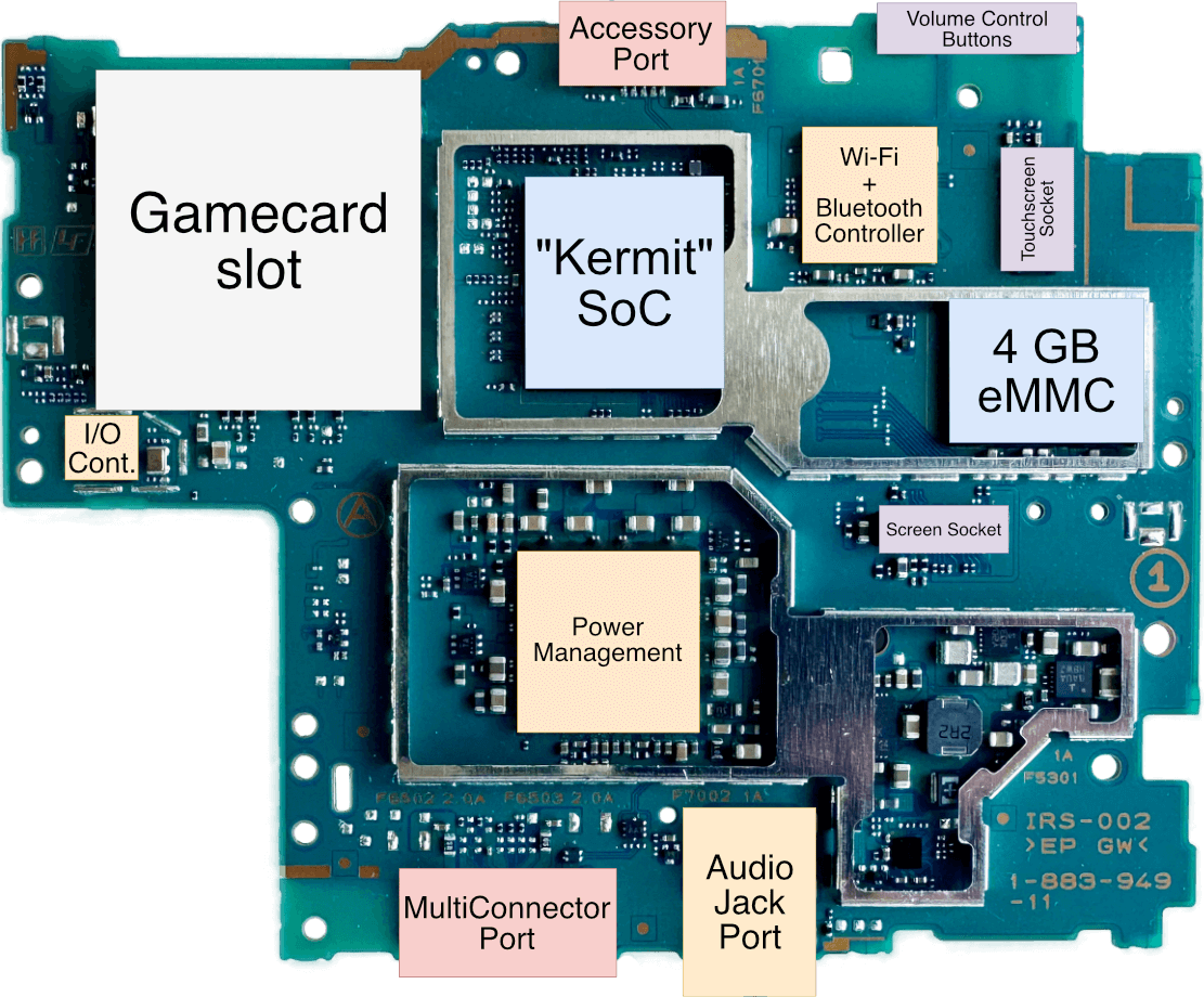
Motherboard
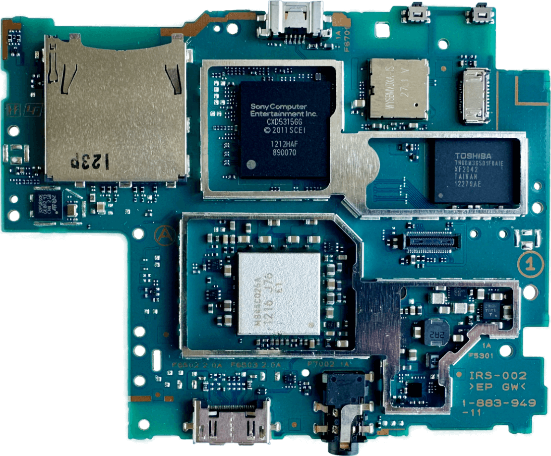
If you yank off the I/O, it becomes a smartphone.
A quick introduction
The PSVita is a noteworthy intersection between the video-game establishment and the rapidly evolving mobile sector. Times have changed, and it won’t be easy for Sony as it faces fierce competition from cheap gadgets that do more than just make phone calls.
The new analysis of this series dives into the contemporary technology behind Sony’s new delivery. Do expect to find recognisable circuitry - perhaps too familiar. Even so, Sony made clear efforts to steer away from any resemblance to the smartphone market.
A new publishing model
Until now, my delivery model involved finishing the whole analysis and then publishing a complete article at once. However, as I continue studying the 8th generation, my articles have considerably grown in complexity. They tend to take almost a year to finish, and the review process has become too cumbersome. Thus, for a change, I’d like to try a new phased approach where I publish by sections instead. This will also make the reviewing stage more efficient.
Having said that, let’s start with the first section.
Models and variants
As the console sat on store shelves, Sony revisited its product strategy multiple times, leading to three variants of the PSVita being shipped throughout its lifecycle:
- The original PSVita (sometimes called the ‘Fat’ model) is the series debut.
- The Slim revision retains the same architecture, but exchanges the OLED screen for an LCD to reduce costs. Furthermore, it doesn’t offer a 3G-capable variant anymore. It does, however, feature a bigger eMMC chip… only 52 MB larger! For some strange reason, that was enough to provide an internal 1 GB memory card. In any case, I’ll explain more in the ‘Games’ section.
- The PlayStation TV is just a Fat motherboard adapted for the non-portable setting. It also exposes a different set of I/O.
As you can see, the information in this article will easily apply to all three models, although I will dedicate extra paragraphs to talk about the puzzling eMMC changes of the last two variants.
CPU
Sony had been an avid adopter of MIPS technology since the original PlayStation. Even at times when SGI/MIPS was losing market share in the late 90s, Sony shipped a successful product carrying MIPS’ revamped line. However, the next decade proved bitter: ARM managed to monopolise the mobile market and MIPS’ adoption only diminished. Thus, Sony ultimately put their faith in an ARM CPU instead, and Toshiba (Sony’s close manufacturing partner) would now play the role of ARM licensee.
The resulting motherboard only houses a handful of integrated circuits, but they package a mix of designs authored by different companies. The main chip is called Kermit [1] (a name borrowed from ‘The Muppets’), it features the largest amount of circuitry, and it’s where the main CPU resides.
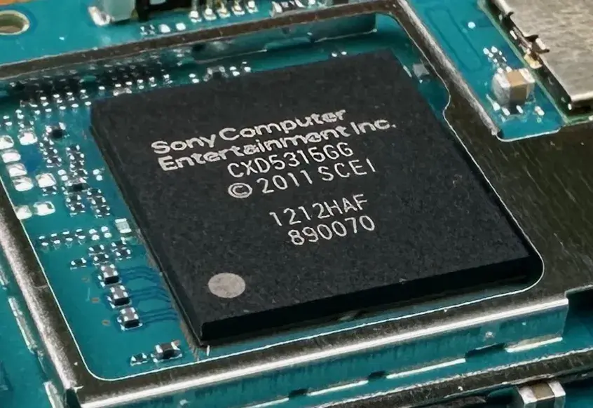
Now, while Kermit is considered a System-On-Chip (SoC), it exceptionally manages to combine large amounts of memory and processors within the same package. This is thanks to Toshiba’s Stacked Chip SoC (SCS) fabrication model [2]. Within it, circuitry is piled on top of others - as opposed to being externally connected side-by-side. The direct consequence is an increase of bandwidth and a reduction of surface footprint, at the cost of a more complex heat dissipation design.
In any case, SCS fabrication enabled Sony and Toshiba to fit cutting-edge technology while maintaining an energy-efficient profile, just look at all the components Kermit houses:
- The main CPU, a quad-core ARM Cortex-A9 MPCore.
- The main GPU, a PowerVR SGX543MP4+ by Imagination Technologies.
- Many accelerators (some proprietary, others off the shelf), including a large DSP, DMA Controllers and security blocks (housing hidden ROM space).
- Around 640 MB of RAM (split into multiple types).
- Last but not least, legacy PlayStation Portable circuitry (the MIPS CPU and the Graphics Engine).
…and throughout this article we’ll take a look at each of those!
The main CPU
Our new study subject is the ARM Cortex-A9 MPCore, a very mature processor from ARM Ltd.
To make this study captivating and help understand all the technological progress since my last analysis of the ARM11 CPU, I’d like to begin with an overview of the new ‘Cortex’ line. Then, a quick look at the Cortex-A8 (the predecessor of the A9). Finally, the novelties of the Cortex-A9.
Continued history
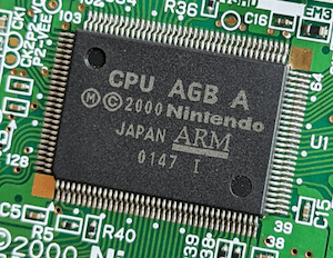
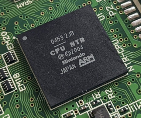
ARM has come a long way since the days of the Game Boy Advance, to recall its significant milestones:
- The ARM CPU was conceived as a replacement of the MOS 6502 CPU for Acorn’s computers, later reaching maturity thanks to Apple’s input.
- The ARM7TDMI paved the way for success in the embedded market. At the same time, competitors across the pond chose to avoid any mobile venture.
- The subsequent StrongARM/ARM9 line granted the company a spot in the performance sector.
- As the competition faded, the new ARM11 line demonstrated this CPU could now partake on 3D applications.
The next achievement would become Cortex: a new brand carrying a revised instruction set and processor line. This time, ARM would adopt practices traditionally found in the desktop/workstation market, eventually coming heads-to-head with Intel’s x86. Curiously enough, Cortex’s marketing strategy is very similar to Intel’s Pentium, in the sense that the name ‘Cortex’ ultimately becomes an ambiguous term to hide the complicated identifications and variants of all its chips.
The Cortex line-up
With the announcement of Cortex as a brand, ARM’s product line diversified into three distinguishable sectors: industrial, performance and embedded. Thus, any Cortex CPU would be fitted into a ‘profile’ (Cortex-R, Cortex-A and Cortex-M, respectively), each targeting one of these markets. For this study, we’ll focus on the Cortex-A line, which focused on performance or ‘applications’ (in other words, user devices); and made a profound impact on smartphones.
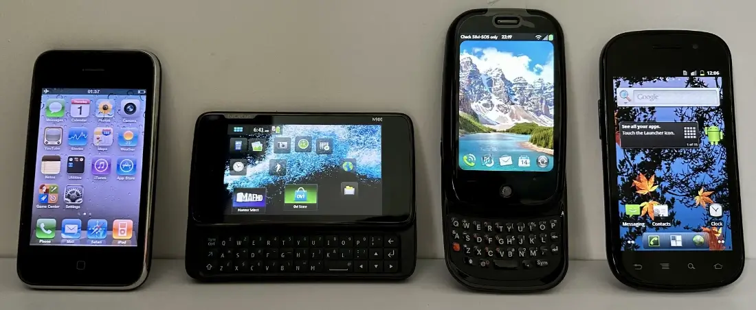
ARM’s first delivery for ‘applications’ was the Cortex-A8 CPU. It shipped in 2005, but it wasn’t until four years later that smartphones started adopting it. The iPhone 3GS, Motorola Droid and Nokia N900 were its debuting flagship carriers. Be as it may, the CPU can’t work by itself, so these devices relied on Samsung and Texas Instruments to package all the necessary modules into a SoC (combining the CPU with the GPU, modem and other I/O).
It’s worth mentioning that the Cortex CPU was also a decisive choice for manufacturers finally making the jump from Intel’s XScale, such as RIM and its Blackberry line. On the other side, certain smartphones like the Toshiba TG01 and the HTC HD2 only adopted Cortex’s technology partially (they implement the same instruction set, but its microarchitecture was designed by Qualcomm instead).
Notice that these devices also coincide with a certain time when users considerably changed their attitude towards smartphones: these were initially trusted for trivial tasks such as text messages and e-mail, but now they were starting to provide access to bank accounts, with only a few years behind bringing contactless payments.
More news
Along the Cortex-A8 came the ARMv7 instruction set. This is the continuation of the ARMv6 ISA by expanding its multi-processing and SIMD capabilities [3].
ARMv7 is the longest-living 32-bit ISA from ARM, but also the last one. Its widespread adoption would still be highly fragmented, mainly due to the split of Cortex into the aforementioned profiles (spawning different subsets of the ISA), existing adoption of the ARMv6 (i.e. the first Raspberry Pi and Nokia’s Symbian platform only supported ARMv6) and the enlargement of Thumb. To avoid making this topic too dense, I’ve dedicated different sections further down to discuss these.
The core
So far I’ve talked about the Cortex-A8, that’s the first Cortex CPU. But the PSVita actually bundles the succeeding CPU, the Cortex-A9 (unveiled two years later, in 2007). It’s curious to see that this console was just a few months apart from the Nintendo 3DS, a console designed with horizontal innovation in mind.
Moving on, the full name of the PSVita’s CPU is ARM Cortex-A9 MPCore. Overall, this means the CPU is a cluster made of multiple Cortex-A9 cores, four in this case. It runs at a clock speed of up to 500 MHz [4], an underwhelming number considering contemporary adopters of the quad-core A9, such as the Samsung Galaxy S III, reached speeds of 1.4 GHz [5]. It’s possible that battery life was the main priority here. Nevertheless, clock speed is not the only decisive measurement, the inner workings of the CPU are as important.
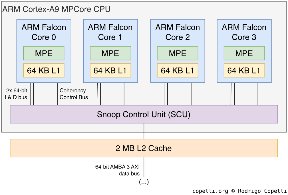
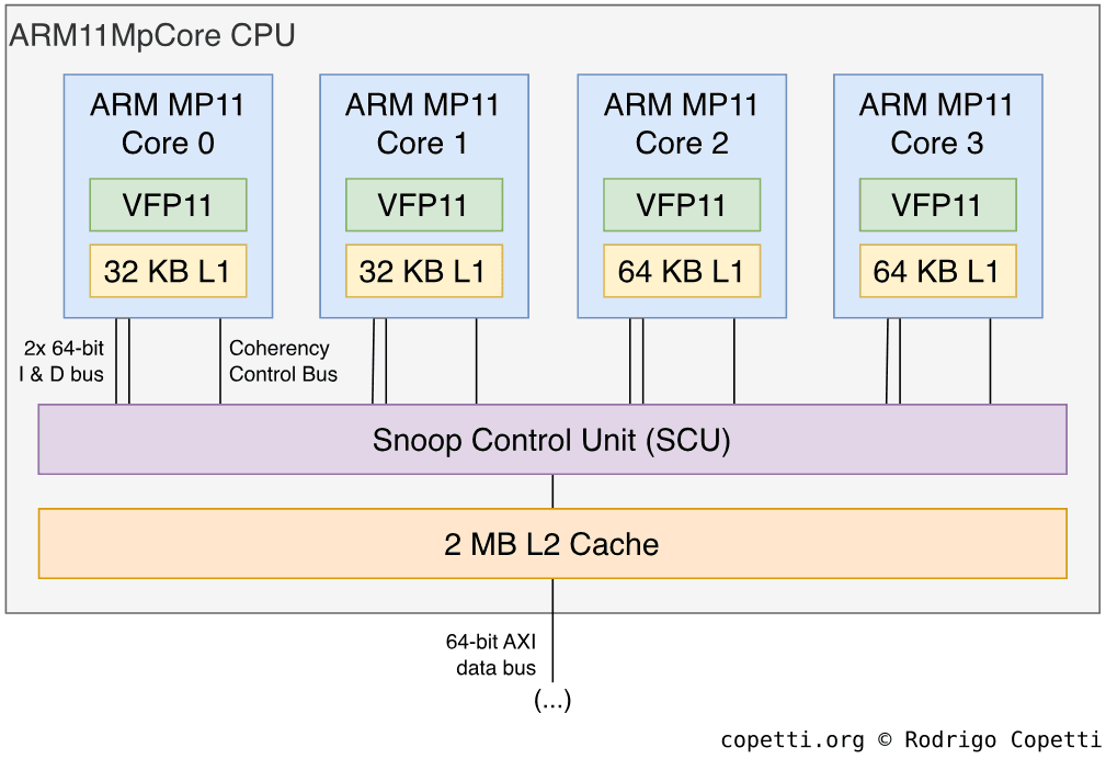
Speaking of which, the new cores share many characteristics with their predecessor, the Cortex-A8, which includes [6]:
- The next-generation instruction set called ARMv7-A, I explain more details further on.
- 64 KB of L1 cache which inherently follows the Harvard architecture. Consequently, it’s divided into 32 KB for data and 32 KB for instructions.
- Data cache coherency among the cores is automatically handled by the Snoop Control Unit, previously featured in the ARM11MpCore.
- 2-issue superscalar: For the first time, ARM has brought instruction-level parallelism. This means that, as long as there are no hazards, the CPU will try to execute two instructions using two separate pipelines. This increases the amount of instructions executed per clock cycle. MIPS and SuperH brought this a decade before, but the two suffered a quick demise, so it’s now ARM’s turn to carry it forward.
- Dynamic branch prediction: The CPU now predicts the execution path by relying on two dedicated buffers while fetching instructions. The first anticipates whether an upcoming instruction will be a branch, and the next buffer maps the previous flow of the program. Finally, the latter is used to predict whether upcoming branches will be taken or not [7].
- It’s worth mentioning that this unit only predicts branching instructions, omitting other optimisation techniques such as conditionals or the
ITinstruction… Maybe that’s a hint about the future of the ARM ISA.
- It’s worth mentioning that this unit only predicts branching instructions, omitting other optimisation techniques such as conditionals or the
- A Memory Management Unit (MMU) with a Translation Lookaside Buffer (TLB). This is already typical on most CPUs.
- TrustZone: A new security subsystem that adds a dimension to the privilege levels of the MMU. It’s implemented on both the hardware level (by segregating components between non-secure and secure groups) and the software level (by executing a secondary and isolated operating system that handles confidential data). The special OS is called Trusted Execution Environment. Furthermore, data transfers carry an extra tag to indicate whether they are secure or insecure transactions [9].
- The OS model of TrustZone reminds me of the isolated SPU of Cell.
- NEON Media Processing Engine (MPE), a new co-processor that carries out vector and floating-point operations. We’ll dive more into it in the next sections.
Now, the Cortex-A9 series (found in the PSVita) improves the original design by applying significant enhancements [10]:
- Multi-core support. This is most evident by looking at Sony’s choice of a quad-core package.
- As a side note, this also explains why portable devices like the iPad 2 and iPhone 4s (both carrying an A9) managed to debut a dual-core CPU.
- Out-Of-Order execution through the use of register renaming. This is a huge step for ARM in further scaling its Instruction level parallelism, considering other chips like PowerPC were forced to abandon it.
- This will also have a profound effect on the evolution of the ARM instruction set. You will see this in a future analysis of the Nintendo Switch.
- A variable-length pipeline, between 8 and 11 stages depending on the operation. The total number may also increase if execution continues in the multimedia co-processor (explained in the next section).
Moreover, Sony customised the package by adding one of ARM’s upgrades called Primelink Level 2 Cache Controller along with 2 MB of L2 cache shared among all cores [11]. Primelink is a flexible cache subsystem which can be programmed with different types of cache associations, from direct mapping to 16-way. If you are curious, years later ARM renamed the Primelink brand to ‘CoreLink’ [12].
The grown-up ISA
The ARMv7 instruction set in the Cortex-A9 features a multitude of extensions. The majority of changes will be in the form of SIMD capabilities and multiprocessing, you’ll notice this when we take a closer look into the novelties of the ARMv7.
A quick glance
ARMv7 is a superset of the ARMv6 ISA. Its additions can be grouped into four areas: VFPv3, NEON, Security Extension and multi-processing. I explain each further down.
Moreover, the alternative Thumb ISA (previously enhanced with Thumb v2) has undergone a major revision called Thumb-2. Truth to be told, it already debuted on embedded ARMv6 CPUs (implementing the ARMv6T2 variant), but it has now become a standard on the Cortex-A line.
On the other side, it’s worth mentioning that ThumbEE, the successor of the deprecated Jazelle, has been left unused or even excluded from many Cortex-A CPUs. Surprisingly enough, Kermit’s Cortex-A9 CPU happens to implement ThumbEE and Jazelle [13], but I don’t think any application takes advantage of these. If you want an idea of its adoption back in the day, let me tell you that Dalvik (Android’s Java interpreter, to put it simply) didn’t even bother using Jazelle/Thumb-2EE at all. That tells you the general attitude towards ARM’s Java efforts.
Overshadowing features
Back to the interesting bit, Thumb-2 is a significant revamp of Thumb because it adds 32-bit instructions [14]. Considering Thumb originally only bundled 16-bit opcodes, the new revision has now filled all the gaps when compared to the master ISA (ARM). Going forward, in contrast with ARM, Thumb-2 offers greater density and is only missing the conditionals. Even so, Thumb-2 manages to bridge this functionality by including an exclusive IT instruction.
Nevertheless, Thumb’s renovation unfortunately means more fragmentation and confusion, eventually to the point assembler developers can’t decide which instruction set to use. Lucky for them, ARM also devised a specification called Unified Assembler Language (UAL) that aimed to consolidate all ISAs into a single codebase that can target both ARM and Thumb-2 ISAs. This allows programs written in UAL to be assembled for all variants of Cortex CPUs (some of which implement ARM and Thumb-2 while others only support the latter). Behind the scenes, UAL is just the union of ARM and Thumb-2 opcodes, the assembler program then skips opcodes based on the target CPU. For instance, when it comes to writing a branching subroutine, programmers must write the two types of branching opcodes in the same routine (ARM’s conditionals and Thumb-2’s IT instruction) - effectively ‘duplicating’ code. However, the assembler then decides which opcodes to parse based on the target processor.
In the case of using programming languages (C, Objective-C, C++, etc.), the decision is much simpler, compilers default to Thumb-2 for assembly generation [15], mainly due to its efficient code density and rare performance penalties. Thus, smartphone apps and, by extension, applications for the PSVita, are mainly compiled to Thumb-2 instead of ARM.
More accelerators
The most notable component of the Cortex-A9, in particular for the PSVita, is the Media Processing Engine (MPE). This is ARM’s new coprocessor for 3D applications. It’s been engineered in a very convoluted way, however, as it executes two different but related instruction sets:
- The Vector Floating-Point v3 (VFPv3): A continuation of VFPv2 for floating-point capabilities. It’s IEEE-754 compliant and now extended to provide instructions like
VCVT(to convert between fixed-point and floating-point values) andVMOV(to transfer values between the CPU and the FPU register file). This is helpful since the VFP only understands 32-bit and 64-bit floating-point values.- The exact variant included in the Cortex-A9 is called ‘VFPv3-D32’, meaning it includes thirty-two 64-bit registers.
- Even though this ISA contains the word ‘vector’, ARMv7 deprecated the use of the vector instructions and the Cortex-A9 includes none [16]. So much for being called a ‘vector FPU’…
- The NEONv1, also known as ‘ARMv7 Advanced SIMD’, is the real vector instruction set, enabling to operate multiple scalars at once. NEON provides sixteen 128-bit registers, which can be also split into thirty-two 64-bit or 32-bit ‘virtual’ registers. The integers being operated may be as big as 64 bits, while floating-point types can’t surpass 32 bits.
- It’s worth reminding that Sony’s predecessor vector unit provided the immense amount of 128 registers, albeit 32-bit instead. If we do the math, the Cortex-A9 MPCore manages to match that number. Although, only 16 registers are accessible per core, and forget about the matrix-type addressing that made the VFPU special and efficient. On the bright side, perhaps there’s a new optimisation opportunity by having multiple cores compute SIMD instructions in parallel.
NEON and VFPv3 share the same register file, but they’re still considered separate ISAs. Considering ancestral processors like the SH-4 delivered SIMD operations by simply extending its FPU, one can only wonder why ARM ended up producing two distinct ISAs. Well, the explanation is simple: neither is feature-complete. Particularly, VFPv3 doesn’t support fixed-point while NEON is not compliant with the IEEE 754 standard [17]. So, as an intermediate solution, the circuitry was segregated.
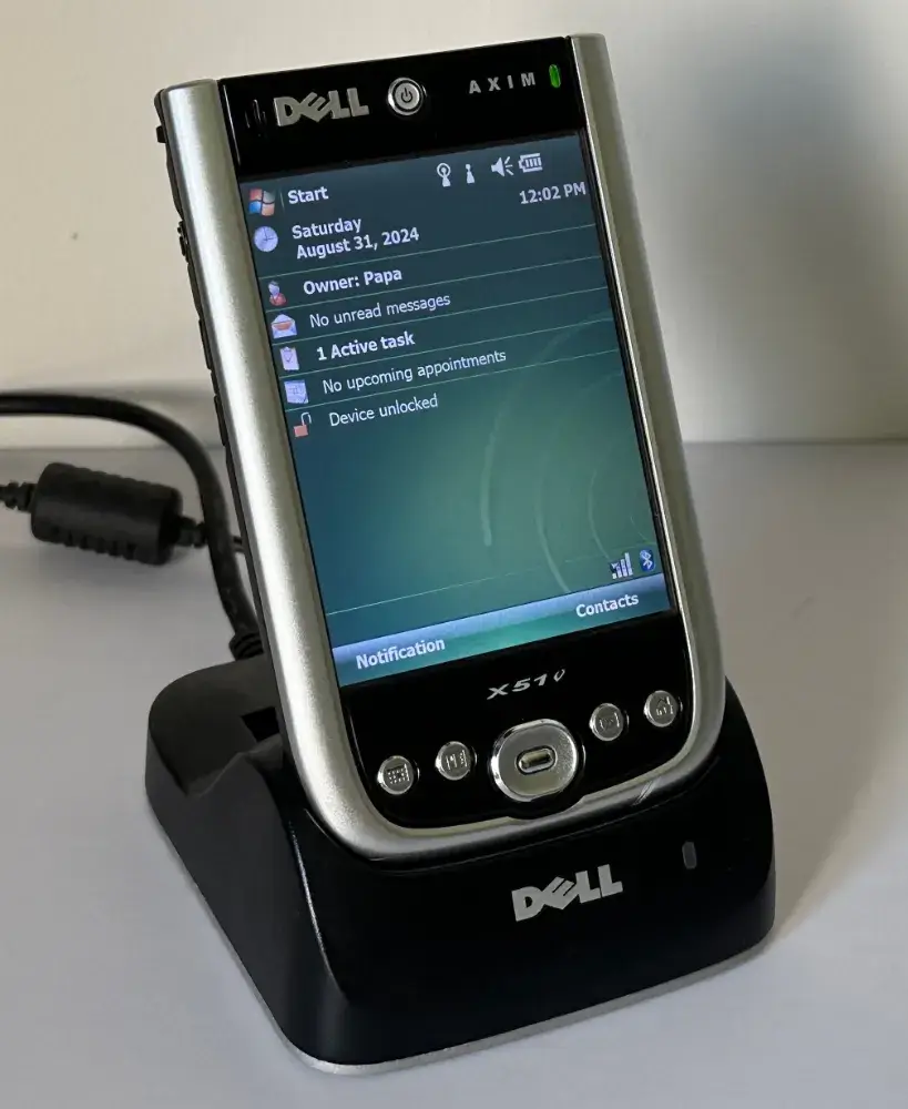
This high-end PDA carried an Intel XScale PXA270 CPU, compatible with the ARMv5 ISA but also bundles proprietary SIMD extensions, which were only available on Intel’s CPU line. This conflicted with ARM’s business model. In response, ARM presented the NEONv1 set.
By the way, this device also houses a PowerVR MBX GPU, which is related to the graphics chip of the PSVita.
All in all, this means the compiler will need to work harder optimising the code, but it still makes you wonder why ARM’s engineers ended up complicating things to absurd levels. In my opinion, I believe NEON was rushed to rapidly counter Wireless MMX (Intel’s proprietary SIMD extension for the XScale, released a year before) as ARM didn’t enjoy seeing Intel bundling exclusive instructions only available on the XScale [18]. This is also complemented by the fact the official documentation on Cortex’s timings was hurried as well [19].
The master bus (or buses)
Another popular product from ARM, the AMBA specification designed for interconnecting components, carries forward with the Cortex-A9. Within its third revision, the AXI protocol was selected for interfacing the cores within the MPCore cluster. Curiously enough, it’s the same choice found in the ARM11 and its well-known adopter, the Nintendo 3DS.
Speaking of which, remember Nintendo’s adoption of the Open Core Protocol (OCP) for communicating with its PICA GPU? Well, that’s also another protocol found in the PSVita, now used for all communications outside the MPCore [20].
Envisioning the future
After the Cortex-A9, the line of succession became increasingly confusing. The Cortex-A series was broken down into four more categories, ranging from the top performer to the most energy-efficient. In doing so, the model numbering of each CPU became absurdly difficult to follow, but I guess it didn’t matter for the end user because these CPUs weren’t sold off-the-shelf!
The next big milestone for ARM will debut in 2011, with the arrival of ARMv8. I’ll talk more about this in a future article about the Nintendo Switch.
The new media coprocessor
Next to the ARM cluster, Sony bundled a large accelerator meant to support gaming-related tasks. Just like the previous Media Engine group, it is completely proprietary and acts as a black box. Programmers are not meant to fiddle with it directly but through the official SDK.
Having said that, this accelerator is called Venezia. This is a complete and separate CPU package designed by Sony’s close partner, Toshiba, for image and sound processing [21]. With functionality closer to a Digital Signal Processor (DSP), Venezia was also sold as a synthesisable chip for multimedia appliances (i.e. DVD players) [22]. Consequently, Sony selected it to accelerate multimedia tasks, so you could say it’s the spiritual successor of the Media Engine.
Architecture of Venezia
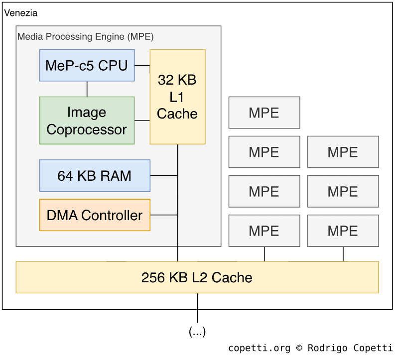
Similarly to the MPCore, Venezia is a cluster, this time made of eight ‘Media Processing Engine’ (MPE) cores operating at 266.7 MHz. Notice that its naming confusingly overlaps with ARM’s vector accelerators, but they are different silicon. That being said, each of Toshiba’s MPEs houses [23]:
- A proprietary ‘Media-embedded Processor’ (MeP) CPU. Particularly, a fifth revision called ‘MeP-c5’. This features a 32-bit RISC-based architecture.
- 32 KB L1 cache, split into 16 KB for instructions and 16 KB for data.
- 64 KB of general-purpose memory. This is where the MeP CPU executes its main program.
- A DMA controller for transferring between internal and external memory.
- An ‘Image Processing’ co-processor named ‘IVC2’ that executes 64-bit SIMD instructions. It can operate different packs of data, from eight 8-bit integers to two 32-bit ones.
- The IVC2 provides two 256-bit accumulator registers, which combined with other capabilities, it allows to compute two operations at the same time.
The cluster also features 256 KB of L2 cache, but its main selling point is found in its instruction set, which is based on the Very Long Instruction Word (VLIW) model. Essentially, a single line can encode multiple instructions at once. In the case of Venezia, three instructions (two for the image coprocessor and one for the CPU) [24]. This requires a very clever compiler capable of packing instructions efficiently, however.
A curious rendition
Interestingly enough, CPU designers once experimented with VLIW implementations back in the 90s when it was thought to be the future of mainstream CPUs. This led to Broadcom’s Firepath, the Transmeta Crusoe and, of course, the Intel Itanium - to name a few. However, the concept didn’t gain traction outside particular uses, as the resulting benchmarks proved disappointing. Thus, interests soon shifted to other parallelism techniques, such as out-of-order execution, which transferred the burden back to the CPU.
Be as it may, Venezia is only accessible through an abstract API called ‘Codec Engine’ [25], which implements different kinds of image and audio encoding/decoding tasks. For instance, there’s an AVC decoding command that decompresses video data encoded with ‘Advanced Video Coding’ (AVC) [26] and outputs an uncompressed stream the GPU understands.
Memory available
Enough about CPU talk! Let’s now take a look at the memory bundled within the PSVita.
As is customary with portable consoles, there are multiple memory types in this system.
Main memory
To start with, at the top of Kermit’s stack, we find a large block that houses 512 MB of LPDDR2 SDRAM and is used as the main working area. In case you are now wondering “I get the ‘512 MB’ part, but what’s with all those initials?”, you’re not alone.
There’s a lot of terminology to unpack here, let’s start by breaking down the ‘LPDDR2 SDRAM’ name into two groups, from right to left, and then inspecting what’s inside each:
- SDRAM means ‘Synchronous Dynamic RAM’.
- Dynamic RAM (DRAM) is the opposite of ‘Static RAM’ (SRAM). DRAM is cheaper to produce but exhibits more latency. That’s why CPU cache is made of SRAM while external general-purpose memory is made of DRAM.
- Synchronous DRAM (SDRAM) means transfers are synchronised on par with the CPU clock, improving its throughput.
- LPDDR2 means ‘Low Power Double Data Rate 2’.
- Double Data Rate (DDR) states that transfers encode twice the information per cycle.
- Low Power (LP) is a novelty here. This is not typical DDR, but a distinct variant called ‘Low Power’. It was initially conceived as a modification of DDR SDRAM, then became its own brand alongside others (as it happened with GDDR). While DDR evolves to increase the bandwidth, new revisions of LP focus on reducing its operating voltage. As you may guess, its main adopters are phones and laptops.
- The ‘2’ at the end signifies it’s the second revision of LPDDR. Its specification was published in 2009 and, among other improvements, it only needs 1.2 Volts to work (compared to 1.35 V for DDR3).
Other memory
There’s another large block of 128 MB of Custom DRAM (CDRAM) predominantly connected to the GPU. ‘CDRAM’ is just an internal name to denote traditional SDR SDRAM which, unlike Double Data Rate (DDR) memory, this one is Single Data Rate. Although, being a dedicated space close to the GPU makes it ideal for intensive graphics operations, which may explain why this block is apparently connected using two 512-bit buses [27].
Apart from that, the SoC also fits an extra ~2.18 MB of SRAM split into different blocks [28]:
- 2 MB named ‘Camera SRAM’.
- 32 KB named ‘SPAD32K’.
- 128 KB named ‘SPAD128K’.
- 4 KB named ‘SceCompatSharedSram’.
- 16 KB named ‘Scratchpad’.
On the other hand, they are all reserved for the operating system, but we’ll discuss them in a later section. By the way, you may want to know that those 16 KB of ‘Scratchpad’ coincide with amount of SRAM also found in the PlayStation Portable, you’ll soon see why.
One last CPU
Last but not least, there’s an additional CPU inside Kermit: The old MIPS32 4k (the same one bundled with the PlayStation Portable) [29]. The intention was to provide backwards compatibility with PlayStation Portable and PlayStation 1 games. That’s the one and only (official) use for the MIPS CPU, with no co-processing capability in place.
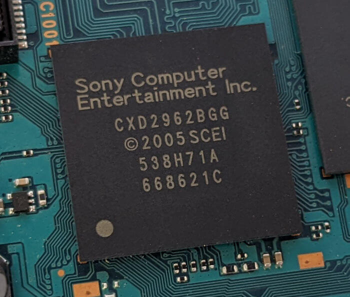
Speaking of backwards compatibility, Kermit doesn’t include the Media Engine [30], although being a black box means that the software doesn’t care about what’s behind the scenes. Thus, the functions of that co-CPU are replicated through Venezia instead.
For the remaining I/O, MIPS is not physically connected to the rest of the hardware, only the Cortex-A9 is. Thus, the PSP emulation software (running on the MIPS CPU) requests services to the ARM CPU by following the ‘Remote Procedure Call’ (RPC) model [31] [32].
Finally, 64 MB of CDRAM are also reserved for this service. Those 16 KB of ‘Scratchpad’ I mentioned before are actually housed within the MIPS CPU [33], and are subsequently allocated to the PSP emulator [34], as original PSP games would expect to find.
Next: Graphics
That’s it for now! In the next part we’ll take a look at VideoLogic’s evolution to become a leading GPU in the mobile market, culminating in their signature PowerVR MBX GPU. Stay tuned for the next delivery!


