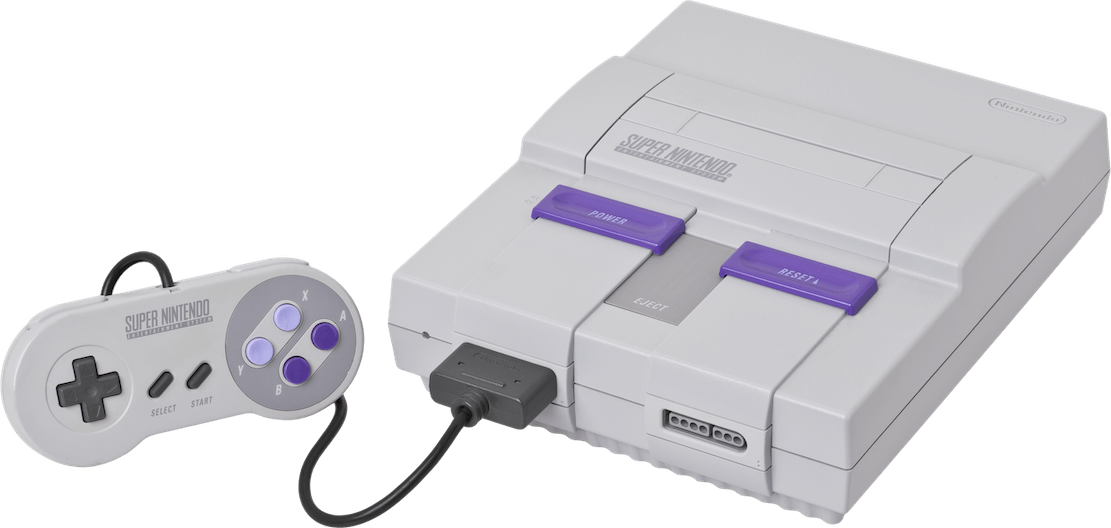
Supporting imagery
Model

Released on 21/11/1990 in Japan and 11/04/1992 in Europe.
Released on 13/08/1991 in America.
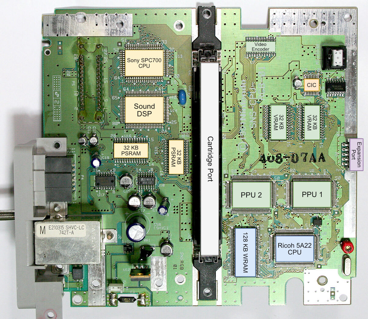
Motherboard
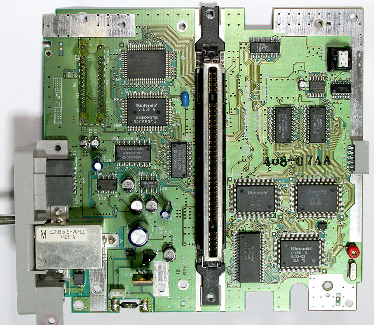
Showing revision 'SNS-RGB-CPU-01'.
Earlier revisions had the Sound Subsystem connected as a daughterboard, later ones unified both PPUs.
Diagram
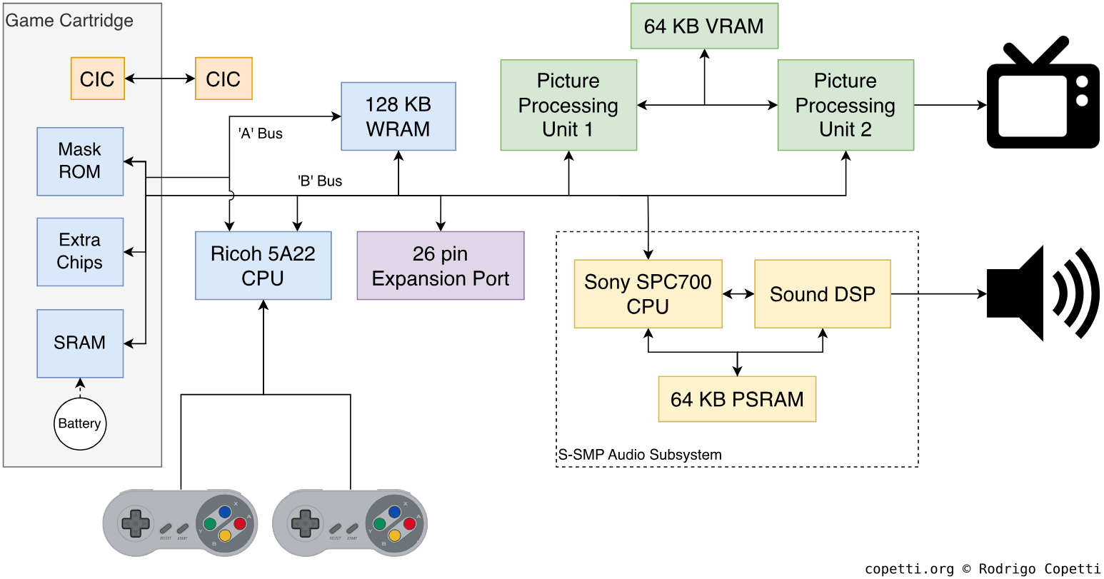
Bus 'A' and 'B' are address buses, the data bus follows the trail of bus 'B' and it's 8 bits wide.
A quick introduction
It seems Nintendo managed to deliver the next generation of graphics and sound without using expensive off-the-shelf components. But there’s a catch: the new console was also designed with expandability in mind. In a world where CPUs are evolving faster than the speed of light, Nintendo ultimately relied on game cartridges to make its console shine.
Models and revisions
Kids across the globe saw this console in various shapes, colours, and names. Nevertheless, the internal differences were less noticeable. As you may already know, due to the spread of analogue standards, models from different regions exhibit variations in their analogue signals (e.g., video output) to accommodate these differing standards. Compared to its predecessor, however, the architectural differences are less pronounced. For instance, on this occasion, Nintendo did not include exclusive circuitry for audio expansion, which significantly impacted the quality of games across regions.
The company did ship hardware revisions during its lifespan, but their main purpose was to reduce the number of dedicated components on the motherboard, thereby lowering manufacturing cost.
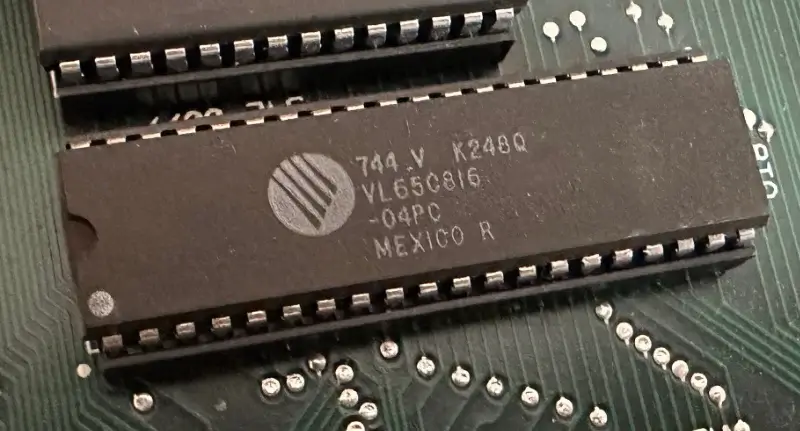
CPU
The Super Nintendo’s choice of processor is a peculiar one. Unlike its competition bundling a fully-fledged 68000, the SNES’ chip is not a radical departure from its predecessor. To recap, the NES employed a modified 6502 CPU, an admired ingredient of late-70s and early-80s computers. Now, to pave the way for the new decade (the 90s), Nintendo opted for a more conservative (and cheaper) solution: the WDC 65C816, a 16-bit extension of the 6502.
Modernising the 6502
The 65C816 CPU originates from Western Design Center (WDC), particularly from Bill Mensch, a former member of the 6502 team (at MOS) and the 6800 team (at Motorola). In 1978, one year after leaving MOS, Mensch founded Western Design Center, a semiconductor company that produces clones of the MOS 6502 with attractive enhancements (e.g., CMOS design, extra opcodes, circuitry fixes, new addressing modes, etc.).
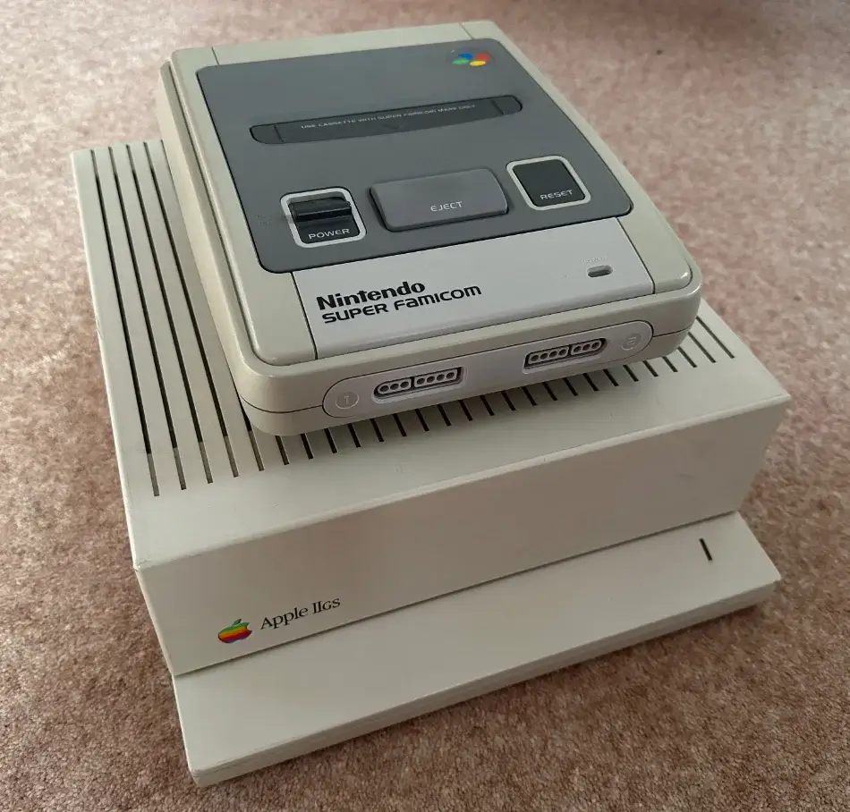
One day, Apple approached WDC to design a backwards-compatible variant of the 6502 that could process larger amounts of data. This resulted in the WDC 65C816 CPU, released in 1983. Curiously enough, Apple encountered many setbacks during the development of a computer that would use the new CPU, until three years later, with the release of the Apple IIGS.
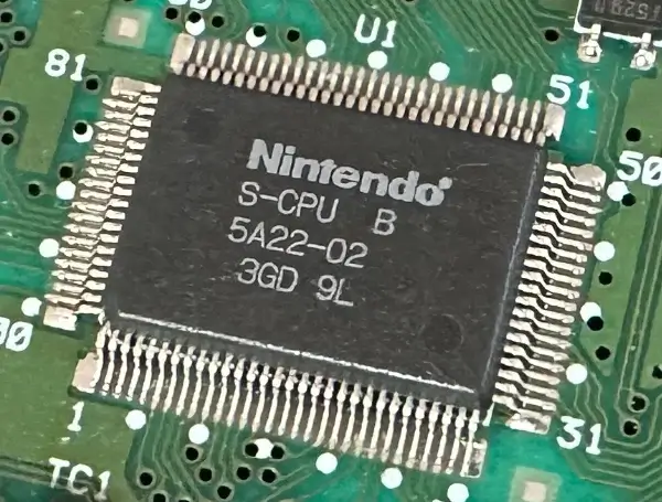
Meanwhile, Nintendo was enjoying a good relationship with Ricoh and their set of bespoke chips for the NES. I haven’t found the exact document outlining what connected Ricoh to WDC, but what I can confirm is that at some point in time, WDC agreed to license their 65C816 designs to Ricoh [1]. Consequently, the latter tailored it to meet the new requirements of the Super Nintendo, it became the Ricoh 5A22 and was exclusively supplied to Nintendo.
The new CPU
As you’ve seen before, the main processor of this console is the Ricoh 5A22, a superset of the 65C816.
Unlike the Apple IIGS, which enjoyed backward compatibility with Apple II software, the Super Nintendo is not compatible with NES games. To be fair, based on the choice of processor, there’s a slight possibility that the SNES was originally planned to be compatible with NES games, who knows.
Moving on, the CPU employs a variable clock speed, reaching up to 3.58 MHz for register operations and dropping to 1.79 MHz when accessing the slowest buses (i.e. the serial/controller port).
Now, to properly understand the functionality of the 5A22, we must first look at what the 65C816 provides:
- The 65816 ISA: The debut 16-bit instruction set of the 65C816. It is based on the 6502 ISA but does not implement undocumented instructions that some NES games resorted to [2].
- The size of instructions can vary between 1 byte (8 bits) and 4 bytes (32 bits), depending on how memory addresses are referenced (a.k.a. the ‘addressing mode’ used) [3].
- The broken BCD mode is functional again (I’m guessing as a consequence of appropriate licensing).
- 10 different modes of operation: Due to a combination of backwards compatibility with the 6502, the return of the BCD mode (missing on the NES), and the ability to switch between groups of 16-bit and 8-bit registers [4], developers can utilise this CPU using different combinations of these.
- Unlike later MIPS CPUs, there isn’t a mixed instruction set with dedicated opcodes for 8-bit and 16-bit words. Instead, the same instruction set is interpreted differently depending on the mode activated.
- For compatibility reasons, the CPU always starts in ‘emulation’ mode (pure 6502), and it is up to the program to switch to a particular ‘native’ mode to enable 16-bit functionality. On a side note, it is amusing how Intel’s x86 still follows the same modus operandi in their modern CPUs.
- Three 16-bit general-purpose registers. This set matches the 6502’s (
X,YandA). However, due to the different modes of operation, these registers can now switch between 16-bit and 8-bit.- Compare this number to the sixteen 32-bit registers the competition offered - quite a contrast!
- 16-bit internal data bus and an 8-bit external data bus: This results in performance penalties when moving values larger than 8 bits across memory (as the CPU requires additional cycles), a common occurrence considering most instructions are 16-bit long. However, the overall impact is alleviated thanks to Ricoh’s DMA units (explained later on) and the variable clock speed.
- 24-bit address space: Allows the CPU to access up to 16 MB worth of memory. This is similar to the Motorola 68000, except the 65C816 obtains its 24-bit addresses by combining extra 8-bit registers (
DBRandPBR) with the original 16-bit addressing lines of the 6502 [5]. Overall, this methodology is similar to housing an internal mapper.
Looking at this, I have to confess that the 65C816 feels excessively cumbersome for little gain. Compared to other offerings such as the Motorola 68000, it is not difficult to conclude why the Apple IIGS remained the only personal computer to adopt the 65C816. Nonetheless, throughout this article, you will see how Nintendo and Ricoh managed to turn the limitations of this CPU into opportunities to revamp its game library.
Ricoh’s additions
In 1983, the 65C816 CPU was conceived as a general-purpose successor of its 1975 ancestor, with all the associated requirements and constraints. Yet, Nintendo planned its console to last throughout the 90s, meaning Ricoh had to step up its game (if you’ll pardon the pun).
First on the list was tackling its arithmetic limitations - the 65C816 lacks dedicated instructions for multiplication or division. As a result, Ricoh incorporated multiplication and division units, enabling the CPU to perform these types of operations via hardware (rather than software). Instead of conventional instructions, they are operated through registers.
The multiplier receives 8-bit numbers and outputs 16-bit ones [6]. Conversely, the divider takes a 16-bit dividend and an 8-bit divisor; and returns a 16-bit quotient along with a 16-bit remainder [7]. Both units only support positive numbers (called ‘unsigned’).
Now, you may be wondering ‘why is this relevant?’. The significance of these additions will become clear when we explore the novelties of the Super Nintendo’s graphics chips (in the ‘Graphics’ section).
Speedy memory access
The second challenge was to increase its data bandwidth. Hence, two exclusive DMAs (Direct Memory Access) were added to move data around without the intervention of the CPU, resulting in faster speeds. For this design to work, regions of memory are referenced using two distinct address buses [8]:
- A 24-bit ‘A Bus’ controlled by the CPU: Connects the cartridge, CPU, and WRAM.
- A 8-bit ‘B Bus’ controlled by the S-PPU: Connects the cartridge, CPU, WRAM, S-PPU, and the Audio CPU.
When setting up a DMA transfer, the origin bus must differ from the destination bus.
Furthermore, the two DMAs are not identical and serve very distinct functions [9]:
- The General-Purpose DMA performs transfers at any time, temporarily halting the CPU until the transfer is finished.
- The Horizontal DMA (HDMA) performs a small transfer after each horizontal scan (while the CRT beam is preparing to draw the next row). This prevents prolonged CPU interruption, but transfers are limited to 4 bytes per scanline.
Finally, the system provides eight channels for DMA transfers, enabling to dispatch up to eight independent transfers at once.
The 16-bit Segmentation Fault
The primitive Open Bus behaviour is also present in this console. Furthermore, there has been speculation about the existence of an internal register called Memory Data Register (MDR), which is believed to store such values [10].
For comparison, the 68000 employs a vector table to handle exceptions, ensuring execution is redirected whenever a fault is detected.
(Lots of) more memory
It’s fascinating to realise how much content the NES managed to display with only 2 KB of RAM. Well, the Super Nintendo now features 128 KB of RAM (still referred to as ‘Work RAM’ or WRAM) - a staggering 6400% increase in general-purpose memory compared to its predecessor.
Be as it may, while the NES enjoyed the fast Static RAM (SRAM) type, Nintendo opted to use Dynamic RAM (DRAM) for the Super Nintendo’s WRAM. Dynamic, in this case, means memory needs to be refreshed periodically. The 5A22 performs this automatically, but during each refresh operation, the CPU is paused. This causes an overall CPU slowdown of roughly 3% [11].
That said, what can developers do with this memory? Anything they desire, really. WRAM is used to store variable data for the game. The more space available, the greater the amount of information that can be stored and processed (thus, reducing reliance on cartridge hardware).
However, as the following sections will demonstrate, the Super Nintendo is a fairly complex machine (albeit its ‘simplistic’ CPU). I tend to call this console a ‘collection of mini-computers/subsystems’. Each subsystem may need data from the CPU, meaning programmers may reserve portions of WRAM to process that information - thus justifying the need for 128 KB of memory.
Graphics
After everything discussed so far, let me tell you that the graphical subsystem of this console is a true feat of engineering. Given its constrained CPU, one might assume the SNES could never cast a shadow on its competitor, which boasts a ‘32-bit’ Motorola 68000. Yet, Nintendo and Ricoh engineers devised clever tricks that exploit the behaviour of CRT displays, effectively expanding the console’s capabilities without the need for expensive, state-of-the-art components.
Before diving deeper into this topic, I strongly recommend reading the NES article first, as it introduces key concepts that will be revisited here.
Design
As with any other console of its generation, the Super Nintendo draws graphics using 2D tiles (8 x 8 pixels). The NES initially achieved this through it signature Picture Processing Unit (PPU), which beams the image in sync with a CRT screen. The Super Nintendo follows suit but incorporates more sophisticated techniques to obtain richer results.
The chipset
The Super Nintendo houses two different PPU chips that constitute the graphics subsystem, collectively known as the Super PPU or ‘S-PPU’.
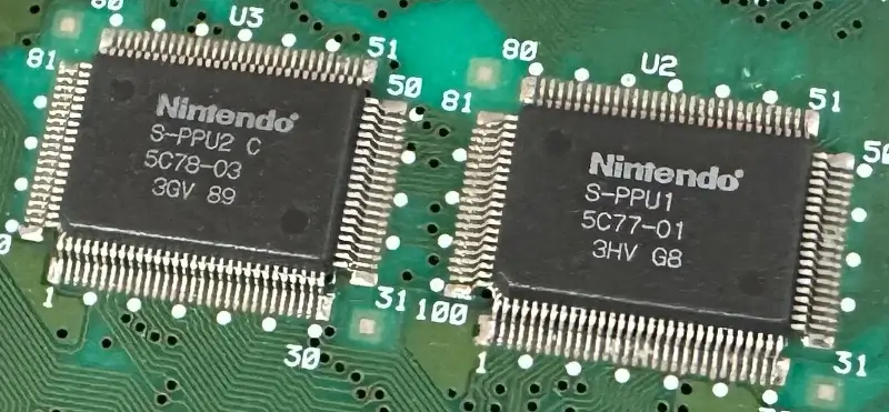
Each PPU package serves specific functionality [12]:
- PPU 1: Renders graphics (tiles) and applies transformations such as rotation and scaling.
- PPU 2: Provides visual effects, including windowing, mosaic, and fading, over the rendered graphics.
This separation, from a programming perspective, is redundant, as both chips are effectively treated as a single unit.
Display modalities
The NTSC system outputs a standard resolution of 256 x 224 pixels at ~60 Hz [13]. The European variant, adhering to the PAL specification, outputs 256 × 240 pixels at ~50 Hz. Be as it may, most games do not utilise the additional pixels and instead display a letterbox (black lines).
Now, here’s the tricky part: traditional TVs have an aspect ratio of 4:3. Yet, if you do the math, the Super Nintendo’s output resolution has an aspect ratio of 8:7. Consequently, once the image is beamed on the TV, it looks horizontally stretched, resembling a 292 x 224 pixels frame instead (in the case of the NTSC variant) [14]. Put simply, pixels on the Super Nintendo have an aspect ratio of 8:7, rather than being ‘perfectly square’.


The reasoning behind Nintendo’s deviation from the standard aspect ratio boils down to cost. You will soon see that the S-PPU is very rich in functionality, but not fast enough to render everything at the pace of the CRT beam [15]. Rather than adding more circuitry to the board, Nintendo opted to shorten the width of the visible image, allocating extra space for the horizontal blanking period instead.
Nevertheless, some games like ‘Chrono Trigger’ account for this factor by intentionally using squashed shapes, which then look correct after being stretched by the TV. This, however, remains an exception, since the majority of games take no extra measures to compensate for this effect.
Organising the content
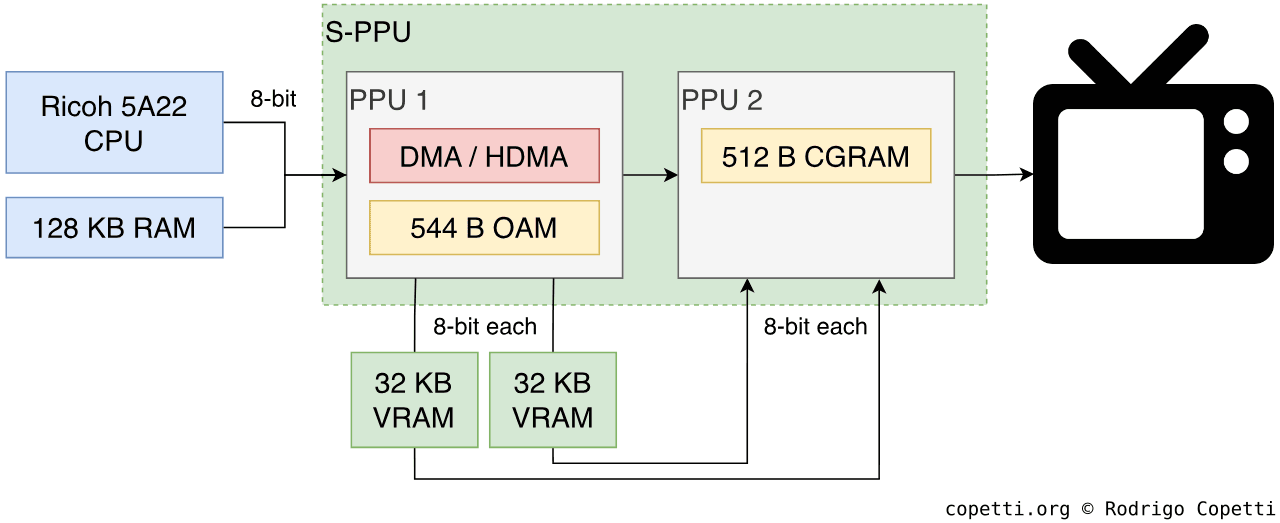
Due to cost and performance reasons, graphics data is distributed across three memory regions:
- 64 KB VRAM (Video RAM): Stores tiles and maps (tables) used to build background layers.
- 512 B CGRAM (Colour Graphics RAM): Fits 512 colour palette entries, with each entry occupying a word (16 bits).
- 544 B OAM (Object Attribute Memory): Contains tables referencing 128 tiles that will be used as sprites, along with their attributes.
VRAM is implemented using two 32 KB chips, each accessed simultaneously via a separate 8-bit bus. This allows the PPU 1 to fetch 16-bit values per cycle, making it particularly efficient for retrieving multiple consecutive pixels in real time [16]. Additionally, each VRAM chip is connected to a dedicated 16-bit address bus, rather than a shared one. This will prove useful when the PPU 1 needs to switch to alternative memory arrangements - something we’ll explore in more detail when we talk about ‘Mode 7’.
Constructing the frame
Let’s now see how a frame is rendered on the console and subsequently displayed on TV. For demonstration purposes, Super Mario World will serve as example.
Tiles

Just like its predecessor, the S-PPU uses tiles to build sophisticated graphics. Although, there are significant improvements compared to the original PPU:
- Game cartridges are no longer wired to the PPU, meaning tiles must first be copied to VRAM (similar to Sega’s Mega Drive). This is where the DMA unit becomes very handy.
- Tiles are no longer restricted to their traditional dimension (8x8 pixels) - they can now be up to 16x16 pixels wide.
- When tiles are stored in memory, these are compressed based on colour depth (in other words, the number of colours per pixel). The unit of measurement for this is bpp (bits per pixel). The minimum value is 2 bpp, meaning each pixel occupies two bits and has only 4 colours available. The maximum is 8 bpp, allowing for 256 colours per pixel (at the expense of consuming a full byte of memory).
Background


The Super Nintendo can generate up to four different background planes. Using either 8x8 or 16x16 tiles, blocks are made of 32x32 pixels (2x2 tiles). That being said, each background layer can extend up to 1024x1024 pixels in size (32x32 tiles). The region in VRAM where these layers are configured is called Tilemap, and is structured as a table (continuous values in memory).
Each Tilemap entry contains the following attributes:
- Vertical and horizontal flip values.
- Priority (either
0or1). - Palette reference from CGRAM.
- Tile reference.
As always, these planes are scrollable. However, the number of features available - such as colour depth, number of layers, independent scrolling regions, and size of selection - depends on the Background Mode activated on the S-PPU, which brings us to the next section…
Modes
The S-PPU provides many operations for backgrounds, but these cannot be chosen arbitrarily. Instead, programmers must choose from eight background modes, each offering a distinct set of features [17]:
- Mode 0: 4 layers with 4 colours each.
- The colour palette is particularly bland, as this mode prioritises the highest number of layers.
- Mode 1: 2 layers with 16 colours each + 1 layer with 4 colours.
- One layer can be split into foreground and background.
- This is the most commonly used mode.
- Mode 2: 2 layers with 16 colours each.
- There is an extra effect available: layers can have each of their columns scrolled independently (similarly to the Game Boy wobble effect but applied vertically).
- Mode 3: 1 layer with 256 colours + 1 layer with 16 colours.
- Colours can be defined using RGB values instead of referencing CGRAM.
- Mode 4: Mode 2 and 3 combined (Column scroll + RGB colour mapping).
- The first layer supports 256 colours, while the second is limited to just 4 colours.
- Mode 5: 1 layer with 16 colours + 1 layer with 4 colours.
- The selected area features an outstanding resolution of 512 x 224 pixels, which will be horizontally squashed to fit on the screen (the final output remains 256 x 224 pixels!). This comes at the cost of rendering 16 x 8 pixels tiles as 8 x 8 ones, and 16 x 16 pixels tiles as 8 x 16 ones.
- Furthermore, the vertical resolution can be extended by activating interlacing, reaching 512 x 448 pixels, which now maintains correct proportions with the output frame. In exchange, interlacing applies the same squashing effect to tiles - this time vertically. This is useful when displaying larger amounts of information (e.g. multiplayer or split-screen).
- Mode 6: A combination of Mode 2 and 5 (high resolution + column scrolling), though it is restricted to a single layer with 32 colours.
As you can see, programmers can now decide whether to prioritise colour depth, number of layers, special effects, or resolution.
Sprites
A dedicated memory region called Object Attribute Memory (OAM) stores a table with references of up to 128 sprites, each with the following properties [18]:
- Size: The S-PPU can combine up to 16 tiles into a 4x4 tile quadrant to build a sprite.
- Tile references: Specifies the tiles used to draw the sprite.
- Screen position: Only sprites within the visible area will be rendered.
- Priority: Since multiple layers overlap, the graphic with the highest priority will be shown. Priority is also determined by the background mode in use.
- Colour palette slot: Allows selection from 9 palette slots in CGRAM.
- X/Y Flip: Enables horizontal and vertical flipping.
The S-PPU can render up to 32 sprites per scanline; overflowing this will only make the S-PPU discard the ones with the lowest priority.
Result

The S-PPU renders each scanline on-the-fly, first processing the relevant portion of each layer and then mixing them.
One of the key constraints of NES games was that graphical updates could only occur during V-Blank - the brief interval when the CRT beam was returning to the starting point provided a reasonable time frame to reshuffle some tiles without breaking the image.
Well, now thanks to the enhanced capabilities of the SNES, this limitation now takes on a different meaning.
You see, because the new DMA/HDMA units enable programmers to perform memory transfers without waiting for V-Blank [19], games can now update tiles, colours, and registers without waiting for the entire frame to be drawn. In fact, the possibilities extend even further: since games can now modify S-PPU settings mid-frame, it becomes possible to activate different background modes at different stages within the same frame, unlocking new and original game designs!
That feature
Truth to be told, I still haven’t mentioned the most important characteristic of this console…


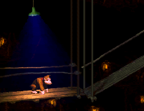
The first quarter of scan-lines uses another mode to simulate distance, Mode 7 starts at the second quarter (this is possible thanks to HDMA).
Introducing Mode 7, yet another background mode - but this time, with a completely different way of working. While it can only render a single 8 bpp background layer, it provides the exclusive ability to apply the following affine transformations on that plane [20]:
- Translation.
- Scaling.
- Rotation.
- Reflection.
- Shearing.
Mode 7 is controlled via a rotation matrix, which alters its parameters. Without delving into linear algebra, depending on the desired effect, the CPU must perform some trigonometric functions (sine and cosine) to populate the entries of this table accordingly. This is computationally expensive for the 65C816, even when using fixed-point precision. For this reason, with the 5A22, Ricoh integrated multiplication and division registers to offload some cycles.
By the way, you may notice that the list of transformations does not mention perspective, despite its presence in the example game, F-Zero. This effect is achieved by adjusting the rotation matrix at each HDMA call, creating a pseudo-3D effect in the process. This should give you an idea of just how versatile the S-PPU truly is!
Finally, due to the use of affine transformations, it is no longer beneficial to fetch adjacent pixels from VRAM. So, to maintain acceptable bandwidth, the memory map is restructured in a way that benefits the new pipeline. Thus, the first VRAM chip stores the Tilemap (where tiles are referenced), while the second stores the Tileset (where tiles are stored). Considering entries in both tables are 8 bits long, this setup allows the PPU 1 to retrieve references and tiles in a single cycle.
Generous circuits
Since Mode 7 requires additional computations, the PPU 1 incorporates dedicated circuitry to process the rotation matrix. Now, here is the interesting part: it also exposes the registers for developers to access when idle (in other words, when using Mode 0 to 6, or during V-Blank) [21].
The PPU 1’s multiplier is both faster and more capable than the CPU’s, as it accepts 16-bit numbers, both positive and negative (signed).
Reflecting on this 30 years later, I must say this concept is an earlier precursor to computer shaders.
More colour magic
Behind every rich frame is a flexible rendering pipeline. Well, if all the previous advancements weren’t impressive enough, the S-PPU features a versatile colour blender that enables to customise how layers are merged. Unlike other sprite engines with fixed rendering steps, Nintendo’s engineers exposed multiple parameters within the S-PPU’s pipeline, enabling developers to alter how certain pixels of different layers interact to form the final frame.
This functionality is collectively known as Color Math [22], but it is also called ‘Screen Addition/Subtraction’ - despite also supporting division by two. In any case, this paved the way for realistic transparency, dynamic lighting, and other creative effects.
In essence, the process works as follows [23]:
- Internally, the S-PPU houses two rendering pipelines: Main Screen and Sub Screen, where programmers can assign backgrounds layers and the sprite layer to each.
- The Sub Screen can also be filled with a solid colour instead of receiving layers.
- High-resolution modes (Mode 5 and 6) consume the Sub Screen’s resources, preventing Color Math from working in those modes.
- The pixels of both screens can be masked using individual window parameters.
- The S-PPU separately merges the background layers within Main and Sub Screen, respecting the priority of each layer and window settings.
- Finally, the S-PPU lets programmers decide how to merge the content of Main Screen and Sub Screen. It can add or subtract the two screens, and then divide the result by two (achieving transparency effects).
- Division by two is computationally cheap in digital circuits, as it only requires to shift the value one position to the right.
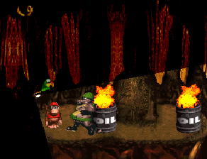
In the second Donkey Kong Country example, Main Screen consists of a single white layer, while Sub Screen contains the rest of the scenery. However, the latter is encoded with inverted colours. At the last stage of the pipeline, the S-PPU applies subtraction and division, producing a correctly coloured frame with transparency effects and enhanced brightness - effectively simulating the torchlight.
Cause of frame drops
On a different topic - what causes games to lag? When the V-Blank interrupt is triggered to allow graphics updates, the game may still be executing heavy code, causing it to miss the V-Blank window. As a result, graphics cannot be updated until the next V-Blank call, and since the frame remains unchanged, this manifests as a drop in frame-rate [24].
Conversely, extensive processing during a V-Blank can block the S-PPU from outputting the video signal, as the bus remains occupied. This can lead to black lines appearing during a scan, though this effect is barely noticeable since the frames refresh 50 or 60 times per second.
A convenient video out
All of the aforementioned advancements would be meaningless unless the console could transmit its picture to the TV through a medium both can understand. With the Super Nintendo, the company debuted some sort of universal-but-proprietary connection called Multi Out, capable of carrying many types of signals at the same time, including Composite, S-Video and RGB [25].
Nintendo bundled a ‘Multi Out-to-Composite’ cable with the console, as composite video was pretty much the common denominator of TVs at the time.
In Europe, however, the SCART port was widely popular, particularly among set-top boxes and VCRs. A major advantage of SCART is its ability to support multiple signal types, allowing AV equipment to select the most optimal format without compatibility issues. As far as I know, only French consumers were offered an official SCART cable that took advantage of the RGB pins exposed on the Super Nintendo [26].
Consequently, Nintendo altered the pinout of its PAL consoles to comply with the SCART protocol, replacing the ‘composite sync’ pin with a 12-volt signal - which instructs the TV to use a 4:3 aspect ratio. Thus, while Multi Out is theoretically universal, RGB cables, if any, are region-specific.
I think the practical benefits of Multi Out have become more apparent in recent years, as it allows users to leverage the RGB output on their modern tellies without tampering with the console’s internals. However, unlike Composite and S-Video, RGB requires an extra ‘sync’ signal. For this, cables can be wired up to capture the sync signal from Composite or S-Video - or for best results, use a dedicated sync line called ‘composite sync’. Unfortunately, as noted earlier, the latter signal is exclusive to NTSC consoles.
Audio
Just like its graphical abilities, the audio department of this console has undergone a significant overhaul. I would argue it even offers the most advanced synthesising techniques of its generation.
Architecture
Some companies partnered with Yamaha, while others devised an in-house solution. Well, Nintendo partnered with Sony - the electronics conglomerate behind the Walkman - to supply a sophisticated synthesiser.
And so, Sony delivered quite an audio subsystem, consisting of the following components:
- The S-DSP: Plays ADPCM samples across eight channels, they are mixed and sent through the audio output. The S-DSP processes samples with 16-bit resolution at a 32 kHz sampling rate, and offers various sound manipulation techniques:
- Stereo Panning: Distributes audio channels to create a stereo soundscape.
- ADSR Envelope Control: Adjusts how the volume changes over time.
- Delay: Simulates echo effects. It also includes a frequency filter to cut out selected frequencies during the feedback (not to be confused with Reverb!).
- Noise generator: Generates pseudo-random waveforms resembling white static.
- Pitch modulation: Allows some channels to influence each other’s pitch, similar to FM synthesis (used by its competitor).
- The SPC700 CPU (also known as ‘S-SMP’): An independent 8-bit CPU that drives the S-DSP and receives commands from the main CPU [27].
- 64 KB of PSRAM: Stores audio data and programs, with the main CPU responsible for loading content into it.
- If ‘Delay’ is enabled, some memory is reserved for feedback data. This is can be dangerous - if not managed carefully, feedback storage could override existing data!
The audio subsystem operates in parallel with the main CPU. When the console powers on, the SPC700 boots a 64-byte internal ROM that sets it up to receive commands from the main CPU [28]. After this setup, it remains idle until instructed.
For the S-SMP to do independent work, it needs to load a type of program known as Sound Driver. This software instructs the chip on how to manipulate raw audio data sent by the main CPU to PSRAM, as well as how to control the S-DSP.
Considering the overall capabilities of this system, most games bundled sound drivers that performed music sequencing. Similar to MIDI, they drive the S-SMP and S-DSP to read sampled instrument data and subsequently play it at different pitches and effects to produce the musical score. This was something that this console excelled at.
As evident, the sound subsystem represented a major leap forward compared to previous generations, but it also posed significant programming challenges. Nintendo only provided one driver, the Nintendo SPC Sound Engine [29]. Along with it, the documentation was infamous for its vague explanations and omission of critical features.
All in all, this forced developers to conduct their own research and derive their own implementations if they wanted extra functionality. Consequently, a wide variety of sound drivers emerged in the market [30], with some uncovering impressive capabilities.
Pitch control
Pitch bending enables to produce distinct notes using the same sample. Well, the S-SMP included a useful bender to alter the pitch in a smooth manner. Take a look at this extracted channel from Mother 2/Earthbound, both examples come from the original soundtrack, however, the first one has the pitch control disabled.
Evolution from the NES
To visualise the evolution of sound from the NES to the Super Nintendo, here is an excerpt from two music scores - one from an NES game and another from its Super Nintendo sequel. Both feature the same composition.
Advanced usage
Here’s a more instrument-rich composition that takes great advantage of pitch bending, echo and envelope.
This combination of techniques allowed the music to only require five channels in total, leaving the other three for sound effects.
Stereo confusion
The S-DSP’s volume controls are organised into signed 8-bits values [31], meaning that volume levels can be set to negative values. But hang on, if ‘0’ represents mute, what happens when the volume is set to ‘-1’? Well, it inverts the signal.
This technique is particularly useful for creating a surround effect, accomplished by setting the stereo channels out of phase - where one channel outputs the normal signal while the other outputs the same signal but inverted.
Unfortunately, abusing this feature results in very unpleasant results, such as the feeling that the music is playing inside your head. For this reason, most SNES emulators bypass this setting altogether.
Additionally, out-of-phase stereo is cancelled out on mono devices, so those games needed to provide a stereo/mono selector to avoid muting their own soundtrack.
Games
To be blunt, the main program is written in plain 65816 assembly and the music driver is written in SPC700 assembly. Needless to say, you won’t find any of the commodities available on 21st-century equipment.
There were, however, some tools distributed by Nintendo, Intelligent Systems and Ricoh to make life easier for programmers, these included [32]:
- Different types of development units, capable of being controlled by a debugger from a host machine (typically running MS-DOS).
- Flashable cartridges (a.k.a. Flashcarts) - not for piracy, but to enable developers test their code on retail units.
- 65816 and SPC700 assemblers.
- Development Manuals explaining from a low-level perspective how this console works. These often included guidelines and norms that developers had to follow to get their game approved by Nintendo (necessary for distribution).
Curiously enough, several game studios - including Argonaut Software, Accolade, and SN Systems - developed custom in-house equipment, often providing more capabilities than the official offerings (e.g. memory editors, floppy disk readers, ISA-based devkits, etc.) [33].
Cartridge configuration
When it comes to accessing the cartridge, things get a lot more confusing compared to the relatively simpler mapping model of the NES. I find it interesting nonetheless, especially for understanding how it could be expanded.
The 65C816 features a 24-bit address bus, enabling to access up to 16 MB worth of data. However, due to the console’s architecture, a portion of the address space is reserved for memory-mapped components. Moreover, the 65C816 only comes with 16 address lines, which are then combined with internal registers to construct a 24-bit address. This is analogous to housing an internal mapper and requiring bank switching to access extra data beyond the boundaries of the address bus. If you explore other systems of the same generation, you’ll find this methodology somewhat familiar.

From top to bottom: LoROM (dual ROM with battery-backed SRAM), LoROM (single ROM with battery-backed SRAM) and LoROM (single ROM)
That being said, when it comes to designing a cartridge, there are many ways to electrically connect the address pins between the ROM and CPU, each utilising bank switching in a different way.
There are two fundamental models that enables accessing up to 4 MB of ROM and 64 KB of SRAM [35], and they work as follows:
- With the LoROM Model, ROM Data is arranged in 32 KB chunks with 128 banks available to choose from [36]. SRAM, though fitting within two banks, is accessible across 15 banks, where ROM data is also present.
- This setup requires frequent bank switching during execution. On the other side, half of the banks are also mapped to WRAM, meaning ROM, SRAM, and WRAM can be accessed without switching banks.
- With the HiROM Model, ROM space is structured into full banks, meaning data is stored in 64 KB chunks across 64 banks. This configuration reduces the need for bank switching, but at the cost of not being able to read ROM, WRAM and SRAM within the same bank.
In both cases, a significant portion of ROM space is mirrored across the leftover area of the CPU’s address space. However, here’s the interesting part: one half of the space operates at ~2.68 MHz while the other can reach 3.58 MHz - but only if the ROM chip supports the higher speed and the CPU’s FastROM flag is enabled [37].
Additionally, cartridges that bundle SRAM must house a MAD-1 (or similar) chip, which performs address decoding. This component is particularly crucial for correctly latching the pins that select between ROM and SRAM chips [38].
Beyond convention
Now, when programmers require more space, derivative models of LoROM and HiROM come into place. Two common variations, known as ExHiROM and ExLoROM, extend the ROM’s addressing space by reducing the mirrored area. Both can access ~7.9 MB of ROM.

Alternatively, and most importantly, LoRom and HiROM can also be adapted to accommodate enhancement chips within the cartridge. These are additional processors that expand the capabilities of the console. To name a few examples of new configurations:
- The MMC model enables bank switching via the local enhancement chip. This was used by components like the S-DD1 or the SPC7110, both function as hardware tile decompressors.
- The Super Accelerator System model was designed for the highly regarded SA-1, a secondary 65C816-based CPU operating at 10.74 MHz with extra functionality. It builds upon the MMC model, incorporating new circuitry for the additional memory-mapped components.
- Two extra configurations - one based on LoROM and the other on HiROM - make way for the DSP series. These chips are derivatives of the NEC µPD77C25 CPU, but running a different program. They provide vector and matrix computations [39]. Various games have used them for affine transformations, graphics decompressing and shortest path calculations.
- The SFX model targets the popular Super FX GSU chip. This configuration maps up to 8 MB of ROM, with 2 MB shared between the main CPU and the Super FX. The rest of the address space includes additional backup RAM and SRAM. Developed by Argonaut, the Super FX is a proprietary processor specialising in 3D surface rendering and 2D affine transformations. The processed graphics are then streamed as tiles for the S-PPU to display. Several notable games leveraged this technology to render 3D models and extend Mode 7 for sprites (as Mode 7 can only transform backgrounds).
It’s difficult to overlook the impact this engineering had on 90s gaming, with many titles surpassing the console’s expectations - and without requiring expansion modules and whatnot. You could say this complicated Nintendo’s plans for a successor console, which may explain the cancellation of advanced games like Star Fox 2.
Anti-piracy / Region Lock
With the Super Nintendo, Nintendo assumed again the sole authority over game distribution. To enforce its policies, the company devised three layers of protection to prevent unauthorised cartridge distribution and circumvention of royalties.
Firstly, the external shape of cartridges is different between regions, so they won’t fit on consoles from different areas. Be as it may, this could be easily bypassed using a third-party adapter.
Secondly, like the NES, this console still incorporates the 10NES protection system to lock out unauthorised distributors. However, the CIC chip was eventually cloned.
As a final layer - specifically designed to combat bootlegging - games included a chain of piracy checks within their program, such as:
- SRAM size verifications: Bootleg cartridges often contain large SRAM blocks to accommodate various games.
- Code integrity checks: A series of checksums embedded throughout the game’s code verify whether the previous SRAM size verification routines have been removed. These checks are dispersed at different stages of the game, making them difficult to locate and remove.
While these measures could be nullified by manually stripping out the routines, this was a time-consuming task. After all, they would be scattered around the game only to upset the player (and eventually make them buy a legitimate copy). Truth to be told, you’ll notice that most ROMs available online have had all their piracy checks removed.
That’s all folks

That game was only released in the states. Luckily, a lad was selling it in Glasgow!


